Semiconductor memory device with selectively connectable segmented bit line member and method of driving the same

a memory device and segmented technology, applied in the direction of information storage, static storage, digital storage, etc., can solve the problems of single-end bit line not being able to write operation, first bit line bl, undesired power consumption, etc., to reduce load capacitance and reduce power consumption

Active Publication Date: 2005-10-04
SAMSUNG ELECTRONICS CO LTD
View PDF7 Cites 7 Cited by
  • Summary
  • Abstract
  • Description
  • Claims
  • Application Information

AI Technical Summary

Benefits of technology

[0009]At least one embodiment of the present invention provides a semiconductor memory device that can reduce power consumption during read / scan operations by reducing load capacitance of a write-only bit line in read / scan operations using single-end bit lines.
[0010]At least one other embodiment of the present invention provides a method of driving a semiconductor memory device that can reduce power consumption during read / scan operations by reducing load capacitance of a write-only bit line in read / scan operations using single-end bit lines.

Problems solved by technology

Due to characteristics of the 6T-type semiconductor graphics memory device, the single-end bit line cannot be used for the write operation.
As a result, undesired power consumption results via the first bit line BL.
For the same reason, undesired power consumption results in the read operation as well.
As a result, MOSFETs M1 and M2 of FIG. 2 are not symmetrical, which has a drawback of low yield.

Method used


Image

  • Semiconductor memory device with selectively connectable segmented bit line member and method of driving the same
  • Semiconductor memory device with selectively connectable segmented bit line member and method of driving the same
  • Semiconductor memory device with selectively connectable segmented bit line member and method of driving the same

Examples


Embodiment Construction

[0019]The present invention will now be described more fully with reference to the accompanying drawings, in which example embodiments of the present invention are shown. In the drawings, like reference numerals are used to refer to like elements throughout.

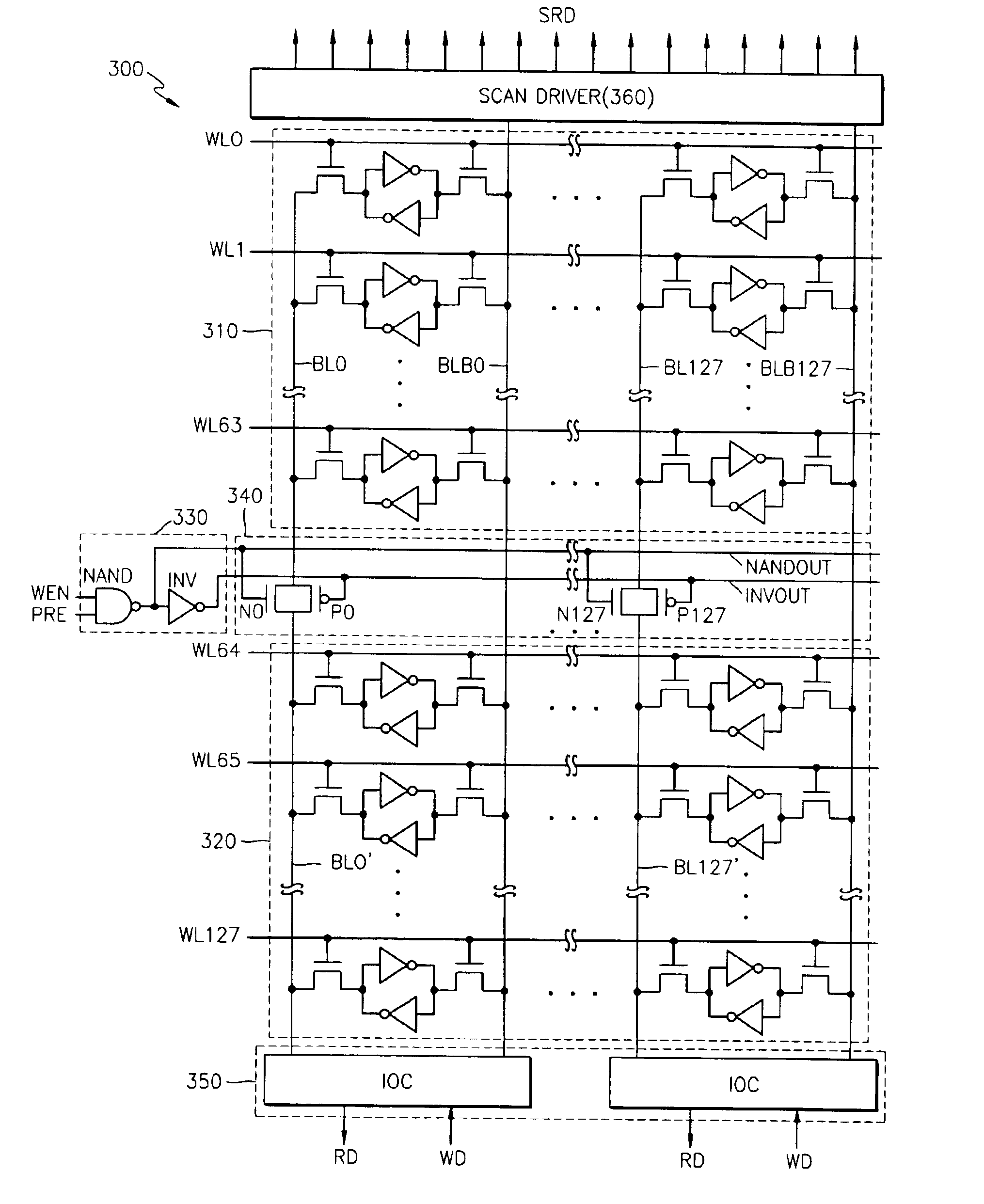
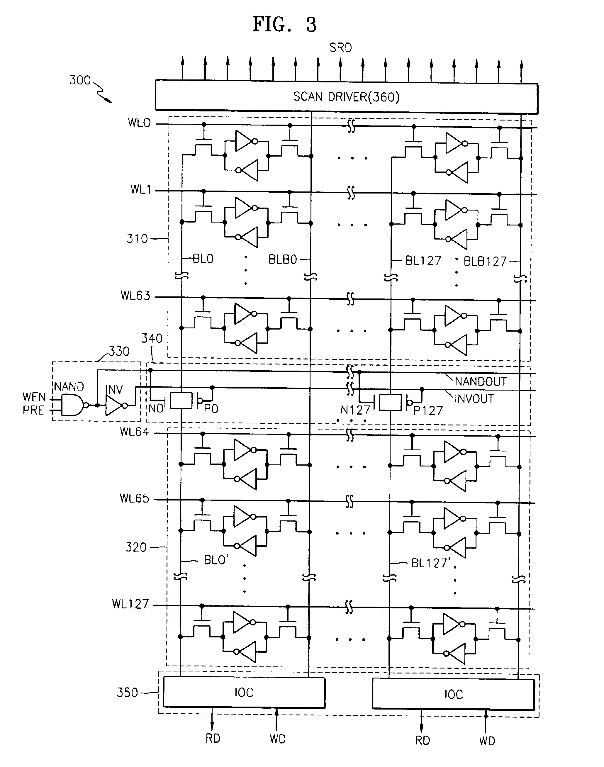
[0020]FIG. 3 illustrates the structure of a semiconductor memory device 300 according to at least one embodiment of the present invention. Device 300 includes a first bit cell array block 310, a second bit cell array block 320, a block division logic 330, a write bit line divider 340, a read / write driver 350, and a scan driver 360. Here, it is assumed that a bit cell array structure has 128 word lines including WL0, . . . , WL127 and 128 bit lines. However, other numbers of word lines and / or bit lines are contemplated; hence, the present invention is not limited by the number of word lines and bit lines.

[0021]First bit cell array block 310 includes bit cells defined by the intersections of a plurality of first bit lines and a plu...


PUM


Abstract

A semiconductor memory device, that reduces load capacitance of write-only bit lines, may include: a first bit cell array block, in which bit cells thereof are defined by intersections of first bit lines and first word lines, the first bit lines being arranged as pairs of first signal lines and second signal lines, respectively; a second bit cell array block, in which bit cells thereof are defined by intersections of second bit lines and second word lines, the second bit lines being arranged as pairs of third signal lines and the second signal lines; respectively; a block division circuit operable to generate and output block division control signals; and a write bit line divider circuit operable to either open-circuit or connect together the first signal lines and the third signal lines, respectively, according to the block division control signals.

Description

CROSS REFERENCE TO RELATED APPLICATION[0001]This application claims the priority of Korean Patent Application No. 2003-34362, filed on May 29, 2003, at the Korean Intellectual Property Office, the disclosure of which is hereby incorporated by reference in its entirety.BACKGROUND OF THE PRESENT INVENTION[0002]Semiconductor graphics memory devices used in liquid crystal display (LCD) products, such as a super twisted nematic (STN) thin film transistor (TFT) LCD that employs an LCD driver integrated circuit (LDI), are of a dual-port type that can perform a read / write operation through one port and a read operation through the other port. These semiconductor graphics memory devices are classified into a 6T type, a 7T type, a 8T type, based on the number of MOS field effect transistors (MOSFET) included in each bit cell. Because the 6T-type has fewer transistors that the 7T-type or 8T-type transistors, it has an advantage of being realized in a smaller chip size. Because of its smaller s...

Claims


Application Information

Patent Timeline
Patent Type & Authority Patents(United States)
IPC IPC(8): G11C7/00G11C8/16G11C7/12G11C8/00G11C8/12G11C11/00G11C11/41G11C7/18G11C11/413
CPCG11C7/12G11C8/12G11C7/18G11C11/41
Inventor SONG, TAE-JOONGKIM, TAE-HYOUNG
Owner SAMSUNG ELECTRONICS CO LTD
Why Eureka
Try Eureka