Artificial intelligence system for track defect problem solving

a technology of artificial intelligence and defect solving, applied in semiconductor/solid-state device testing/measurement, testing/monitoring control systems, instruments, etc., can solve problems such as unwanted electrical bridges, particle blockage of processing chemicals, and serious contamination, so as to facilitate the search for potential solutions

Inactive Publication Date: 2005-10-11
GLOBALFOUNDRIES INC
View PDF24 Cites 46 Cited by
  • Summary
  • Abstract
  • Description
  • Claims
  • Application Information

AI Technical Summary

Benefits of technology

[0015]The defect solution component provides the potential solution(s) to the defect to the defect alert component based, at least in part, upon artificial intelligence technique(s). The defect solution component can analyze the received defect using knowledge of prior and/or known defect(s) (e.g., defect/solution pairs). Artificial intelligence techniq...

Problems solved by technology

These defect(s) may be generated by the fabrication process utilized to produce the mask or reticle as well as during subsequent handling and processing.
Many of the conditions that affect critical dimensions can be difficult to control, often resulting in variations from batch to batch.
For example, contamination can be a serious problem.
Further, the particle can block processing chemicals from reaching portion(s) of the circuitry on the wafer during processing steps.
Some contamination particles can lead to an unwanted electrical bridge from incompl...

Method used


Image

  • Artificial intelligence system for track defect problem solving
  • Artificial intelligence system for track defect problem solving
  • Artificial intelligence system for track defect problem solving

Examples


Embodiment Construction

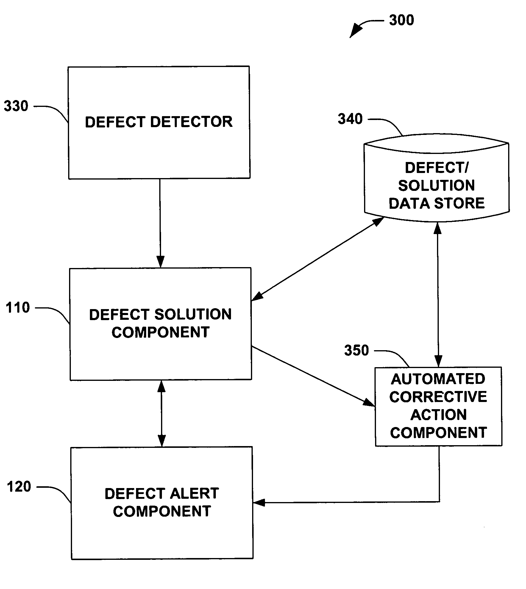
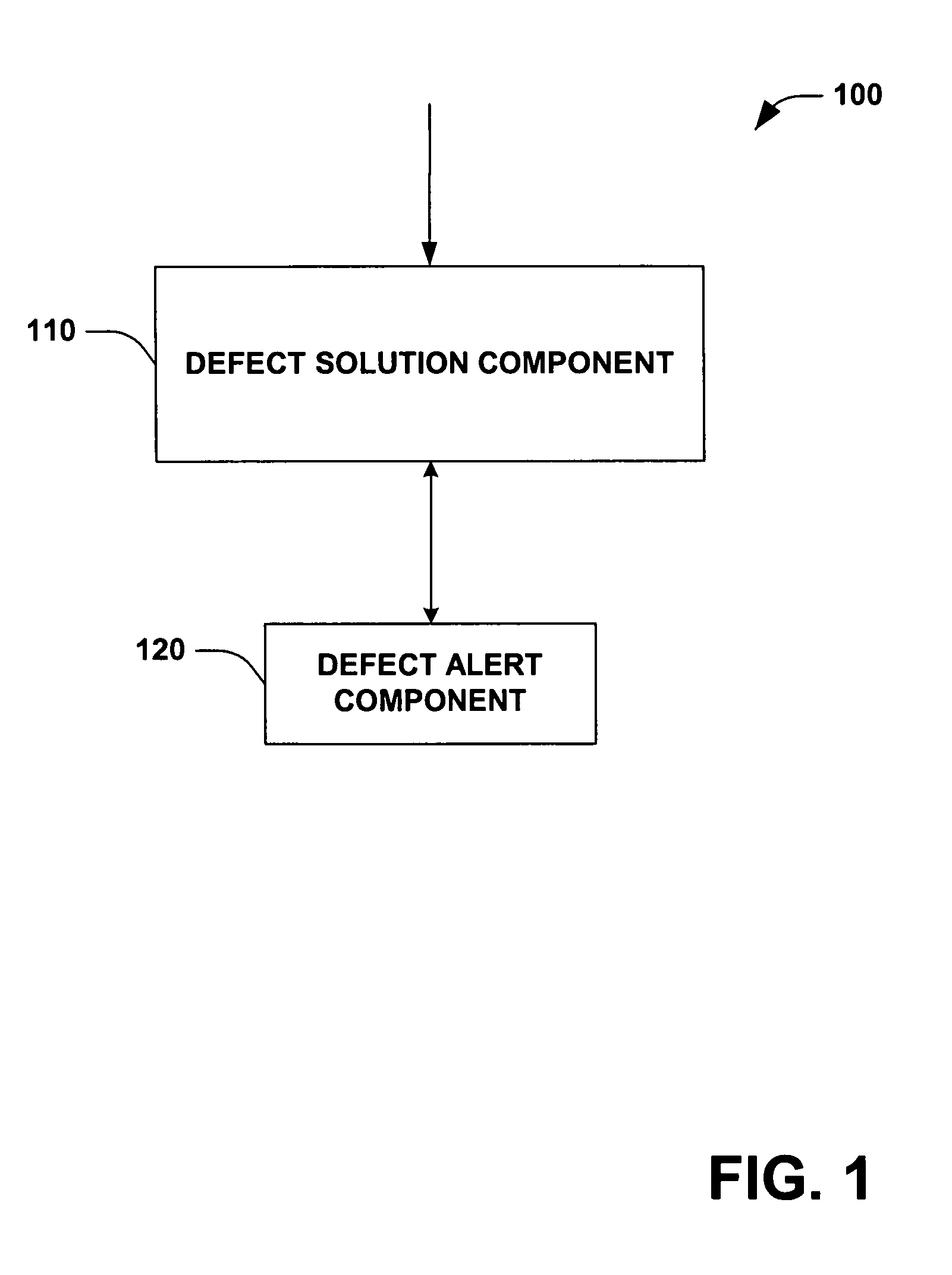
[0030]The present invention is now described with reference to the drawings, wherein like reference numerals are used to refer to like elements throughout. In the following description, for purposes of explanation, numerous specific details are set forth in order to provide a thorough understanding of the present invention. It may be evident, however, that the present invention may be practiced without these specific details. In other instances, well-known structures and devices are shown in block diagram form in order to facilitate describing the present invention.

[0031]As used in this application, the terms “component” and “system” are intended to refer to a computer-related entity, either hardware, a combination of hardware and software, software, or software in execution. For example, a component may be, but is not limited to being, a process running on a processor, a processor, an object, an executable, a thread of execution, a program, and a computer. By way of illustration, b...


PUM


Abstract

A system and method facilitating lithography defect solution generation is provided. The invention includes a defect solution component and a defect alert component. The defect solution component provides potential solution(s) to a defect within the lithography process utilizing artificial intelligence technique(s) (e.g., Bayesian learning methods that perform analysis over alternative dependent structures and apply a score, Bayesian classifiers and other statistical classifiers, including decision tree learning methods, support vector machines, linear and non-linear regression and/or neural network).

Description

TECHNICAL FIELD[0001]The present invention relates generally to semiconductor processing and, more particularly, to a system and method to provide potential solution(s) to defect(s) within lithographic process(es) and / or lithography system(s) utilizing artificial intelligence technique(s).BACKGROUND OF THE INVENTION[0002]In the semiconductor industry, there is a continuing trend toward higher device densities. To achieve these higher device densities there have been, and continue to be, efforts toward scaling down the device dimensions on semiconductor wafers. This continuing trend has also led to advanced monitoring and quality control of the semiconductor manufacturing process.[0003]High resolution lithographic processes are used to achieve small features. In general, lithography refers to processes for pattern transfer between various media. In lithography for integrated circuit fabrication, a silicon slice, the wafer, is coated uniformly with a radiation-sensitive film, the resi...

Claims


Application Information

Patent Timeline
IPC IPC(8): G01R31/26G06F19/00G05B23/02H01L21/66
CPCH01L22/26G05B23/0286
Inventor PHAN, KHOI A.SINGH, BHANWARRANGARAJAN, BHARATHSUBRAMANIAN, RAMKUMAR
Owner GLOBALFOUNDRIES INC
Why Eureka
Try Eureka