
Method of forming chalcogenide comprising devices

a technology of chalcogenide and chalcogenide, which is applied in the direction of semiconductor devices, digital storage, instruments, etc., can solve the problems of data loss, prone to mound on top of these previous bumps

Inactive Publication Date: 2005-10-18
MICRON TECH INC
View PDF218 Cites 68 Cited by
  • Summary
  • Abstract
  • Description
  • Claims
  • Application Information

AI Technical Summary

Problems solved by technology

Volatile storing memory devices result in loss of data when power is interrupted.
Unfortunately when the typical silver electrode material is subsequently deposited, such tends to mound on top of these previous bumps.
Unfortunately, some of the photodeveloper solutions typically used for patterning the top electrode (i.e. tetramethyl ammonium hydroxide) will etch the glass that is exposed.

Method used


Image

  • Method of forming chalcogenide comprising devices
  • Method of forming chalcogenide comprising devices
  • Method of forming chalcogenide comprising devices

Examples


Embodiment Construction

[0021]This disclosure of the invention is submitted in furtherance of the constitutional purposes of the U.S. Patent Laws “to promote the progress of science and useful arts” (Article 1, Section 8).

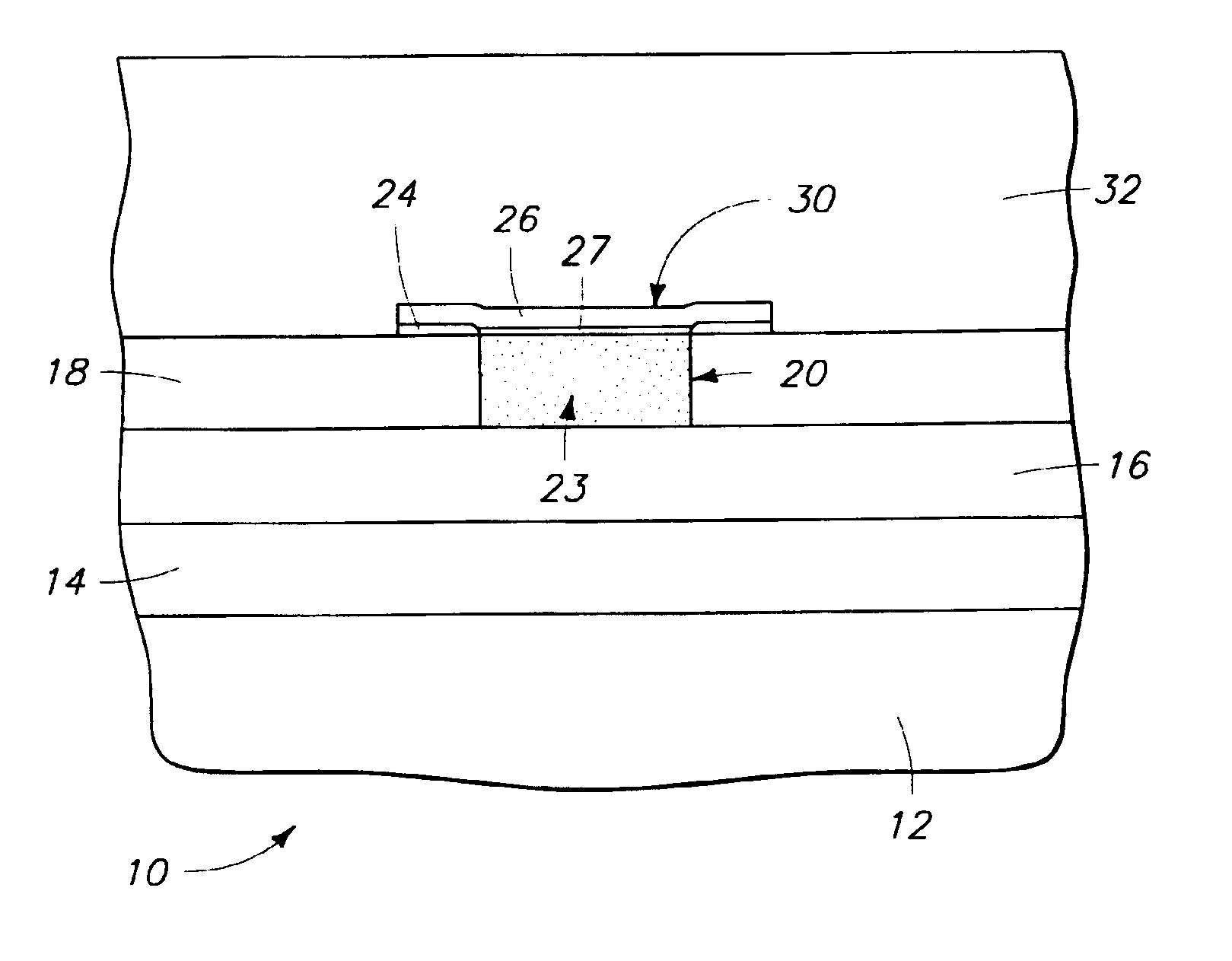
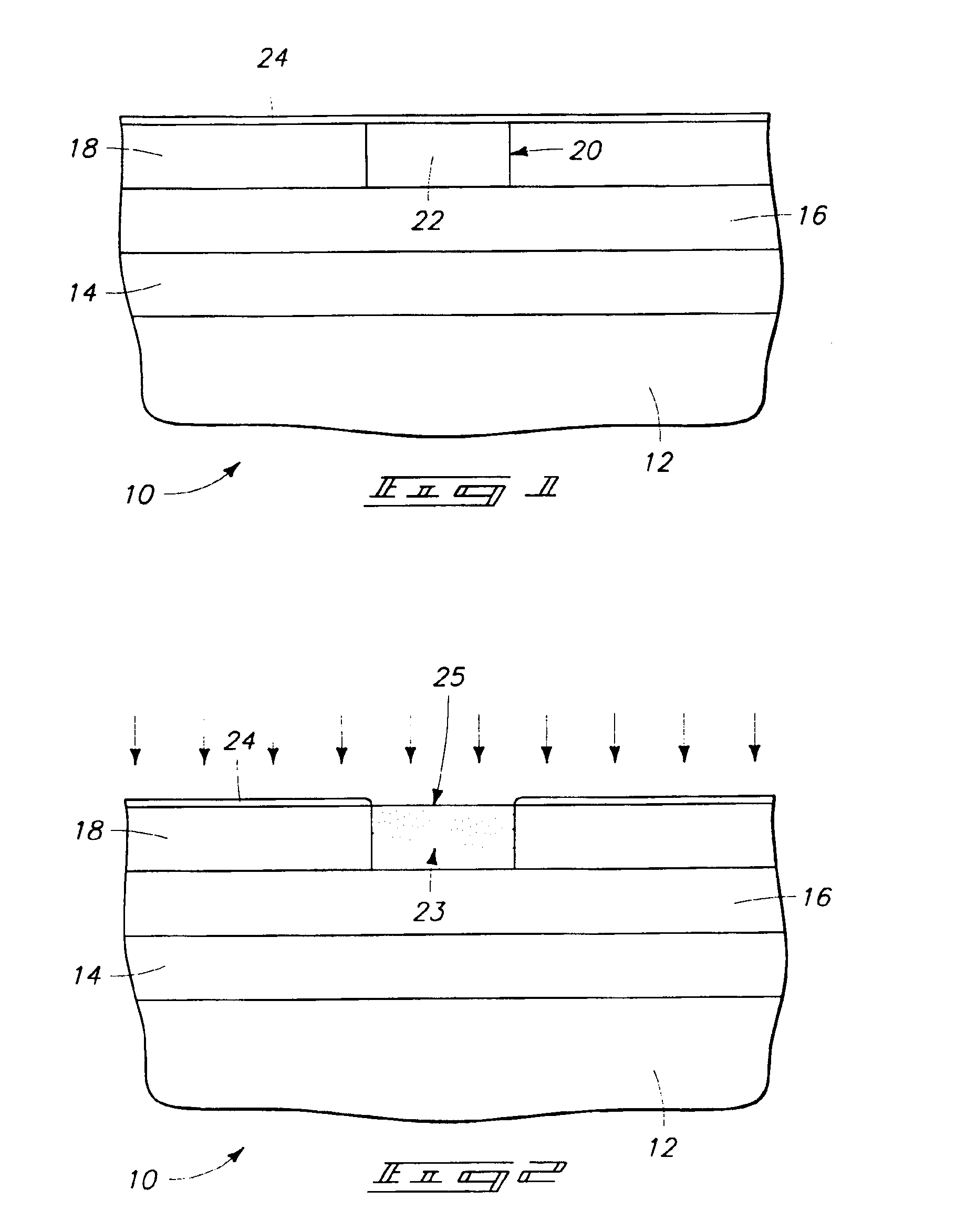
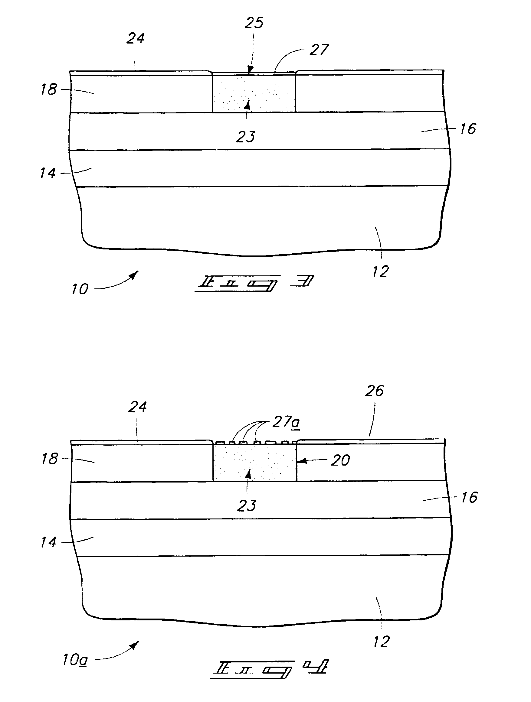
[0022]Referring to FIG. 1, a semiconductor wafer fragment 10 is shown in but one preferred embodiment of a method of forming a non-volatile resistance variable device. By way of example only, example such devices include programmable metallization cells and programmable optical elements of the patents referred to above, further by way of example only, including programmable capacitance elements, programmable resistance elements, programmable antifuses of integrated circuitry and programmable memory cells of memory circuitry. The above patents are herein incorporated by reference. The invention contemplates the fabrication techniques and structure of any existing non-volatile resistance variable device, as well as yet-to-be developed such devices. In the context of this document, the term ...


PUM

PropertyMeasurementUnit
thicknessaaaaaaaaaa
thicknessaaaaaaaaaa
thicknessaaaaaaaaaa

Abstract

A method of forming a non-volatile resistance variable device includes forming a first conductive electrode material on a substrate. A metal doped chalcogenide comprising material is formed over the first conductive electrode material. Such comprises the metal and AxBy, where “B” is selected from S, Se and Te and mixtures thereof, and where “A” comprises at least one element which is selected from Group 13, Group 14, Group 15, or Group 17 of the periodic table. In one aspect, the chalcogenide comprising material is exposed to and HNO3 solution. In one aspect the outer surface is oxidized effective to form a layer comprising at least one of an oxide of “A” or an oxide of “B”. In one aspect, a passivating material is formed over the metal doped chalcogenide comprising material. A second conductive electrode material is deposited, and a second conductive electrode material of the device is ultimately formed therefrom.

Description

TECHNICAL FIELD[0001]This invention relates to methods of forming non-volatile resistance variable devices, for example to methods of forming a programmable memory cell of memory circuitry.BACKGROUND OF THE INVENTION[0002]Semiconductor fabrication continues to strive to make individual electronic components smaller and smaller, resulting in ever denser integrated circuitry. One type of integrated circuitry comprises memory circuitry where information is stored in the form of binary data. The circuitry can be fabricated such that the data is volatile or non-volatile. Volatile storing memory devices result in loss of data when power is interrupted. Non-volatile memory circuitry retains the stored data even when power is interrupted.[0003]This invention was principally motivated in making improvements to the design and operation of memory circuitry disclosed in the Kozicki et al. U.S. Pat. Nos. 5,761,115; 5,896,312; 5,914,893; and 6,084,796, which ultimately resulted from U.S. patent a...

Claims


Application Information

Patent Timeline
Patent Type & Authority Patents(United States)
IPC IPC(8): G11C7/00H01L21/70H01L21/8234H01L33/00H01L45/00
CPCH01L45/085H01L45/1233H01L45/141H01L45/142H01L45/143H01L45/144H01L45/1641H01L45/1658H01L45/1683H10N70/245H10N70/8822H10N70/882H10N70/8825H10N70/826H10N70/8828H10N70/046H10N70/041H10N70/066
Inventor CAMPBELL, KRISTY A.GILTON, TERRY L.MOORE, JOHN T.LI, JIUTAO
Owner MICRON TECH INC
Learn More