Solder bump structure and method for forming a solder bump

a technology of solder bump and solder bump, which is applied in the direction of final product manufacturing, sustainable manufacturing/processing, and semiconductor/solid-state device details. it can solve the problems of increasing ic chip processing speed and ic chip pin count, and unable to meet the demand for new improved technology for fine-pitch wire bonding structures. it substantially impairs device reliability, and the effect of increasing the processing speed of ic chip and increasing the number of ic chip pins

Inactive Publication Date: 2005-11-01
SAMSUNG ELECTRONICS CO LTD
View PDF19 Cites 69 Cited by
  • Summary
  • Abstract
  • Description
  • Claims
  • Application Information

AI Technical Summary

Problems solved by technology

New improved technologies for achieving fine-pitch wire bonding structures cannot keep pace with the demand resulting from increased IC chip processing speeds and higher IC chip pin counts.
Mechanical stresses on the solder bump are a source of structural which can substantially impair device reliability.
Conversely, when the chip cools during an idle state, both the chip and the PCB substrate contract in size.
The larger the crack, the more the interconnection becomes impaired, and device failures can occur when cracks propagate completely through the solder bump structure.

Method used


Image

  • Solder bump structure and method for forming a solder bump
  • Solder bump structure and method for forming a solder bump
  • Solder bump structure and method for forming a solder bump

Examples


Embodiment Construction

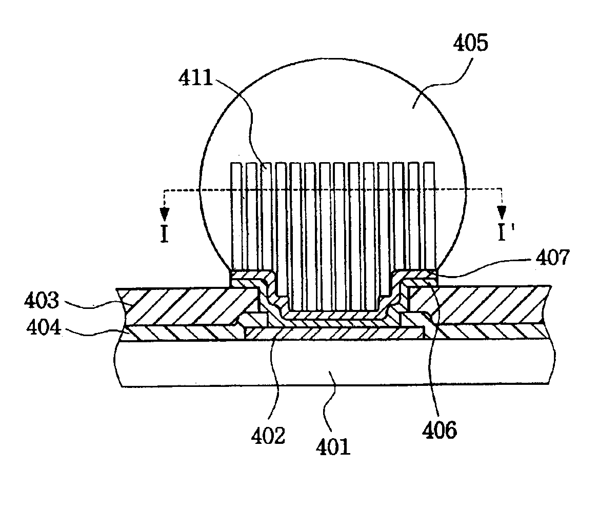
[0027]The present invention is at least partially characterized by the inclusion of one or more metal projections within the solder bump material to form an obstacle which impedes the propagation of a crack within the solder bump material. While the metal projections can take any number of forms, the invention will be described below with reference to several preferred embodiments.

[0028]FIG. 4(a) is a cross-sectional view of a solder bump structure according to an embodiment of the present invention, and FIG. 4(b) a cross-sectional view along the line I-I′ of FIG. 4(a). The solder bump structure includes a contact pad 402 of an electronic device such as an IC chip 401. Preferably, the IC chip 401 is contained a flip chip package or a wafer level package. An opening is defined in one or more passivation layers 403 and 404 which expose a surface of the chip pad 402. Interposed between a solder bump 405 and the chip pad 402 are one or more intermediate layers 406 and 407. The intermedi...


PUM

PropertyMeasurementUnit
widthaaaaaaaaaa
adhesionaaaaaaaaaa
depthaaaaaaaaaa

Abstract

A solder bump structure includes a contact pad, an intermediate layer located over the contact pad, a solder bump located over the intermediate layer, and at least one metal projection extending upwardly from a surface of the intermediate layer and embedded within the solder bump. Any crack in the solder bump will tend to propagate horizontally through the bump material, and in this case, the metal projections act as obstacles to crack propagation. These obstacles have the effect of increasing the crack resistance, and further lengthen the propagation path of any crack as it travels through the solder bump material, thus decreasing the likelihood device failure.

Description

BACKGROUND OF THE INVENTION[0001]1. Field of the Invention[0002]The present invention generally relates to integrated circuit (IC) chips and devices, and more particularly, the present invention relates to solder bump structures of IC chips and devices, and to methods of forming solder bump structures.[0003]2. Description of the Related Art[0004]As integrated circuits (IC's) advance toward higher speeds and larger pin counts, first-level interconnection techniques employing wire bonding technologies have approached or even reached their limits. New improved technologies for achieving fine-pitch wire bonding structures cannot keep pace with the demand resulting from increased IC chip processing speeds and higher IC chip pin counts. As such, the current trend is to replace wire bonding structures with other package structures, such as a flip chip packages and a wafer level packages (WLP).[0005]Flip chip packages and WLP structures are partially characterized by the provision of solder...

Claims


Application Information

Patent Timeline
Patent Type & Authority Patents(United States)
IPC IPC(8): B23K3/06H05K3/34H05K1/11H05K3/24H01L21/60H01L21/288H01L23/485
CPCB23K3/0623H01L24/03H01L24/05H01L24/11H01L24/12H05K1/111H05K3/3436H01L21/2885H01L2224/13078H01L2224/0401H01L2224/05599H01L2224/1147H01L2224/11901H01L2224/13099H01L2224/131H01L2224/13111H01L2224/13144H01L2224/13147H01L2224/16H01L2924/01002H01L2924/01004H01L2924/01005H01L2924/01006H01L2924/01013H01L2924/01022H01L2924/01028H01L2924/01029H01L2924/01046H01L2924/01047H01L2924/0105H01L2924/01078H01L2924/01079H01L2924/01082H01L2924/014H01L2924/14H05K3/243H05K2201/0367H05K2201/0373H05K2201/10674H05K2203/048H01L2924/01024H01L2924/01033H01L2924/01068H01L2924/00014H01L2224/13076Y02P70/50H01L21/60
Inventor OH, SE-YONGKIM, NAM-SEOG
Owner SAMSUNG ELECTRONICS CO LTD
Why Eureka
Try Eureka