Multi-exposure lithography method and system providing increased overlay accuracy

Active Publication Date: 2005-11-01
SAMSUNG ELECTRONICS CO LTD
View PDF5 Cites 2 Cited by
  • Summary
  • Abstract
  • Description
  • Claims
  • Application Information

AI Technical Summary

Benefits of technology

[0018]The invention is directed to multi-exposure lithography systems and methods that provide improved overlay accuracy when using a plurality of sub-images. In general, according to the present invention, methods and systems for performing multi-exposure lithography are optimized to independently correct the overlay according to the sub-layout or sub-image. The overlays are independently corrected according to overlay parameters corresponding to the sub-layout or sub-image so that the overlay accuracy is improved.

Problems solved by technology

However, improvements to the exposure equipment typically do not match the demands of the semiconductor device manufacturers that desire to form finer patterns.
Since semiconductor devices include various patterns on a single layer, existing exposure equipment and methods are not diverse enough to process the various patterns that may exist for highly integrated devices.
Improving the exposure equipment is time consuming and costly with respect to the manufacture of the semiconductor devices.
However, as the overlays of every pattern become important due to reduction of the design rule of the devices, the above-described method becomes inappropriate.
Accordingly, the method of using the average value of the overlay offsets to determine an overlay parameter is inappropriate.

Method used


Image

  • Multi-exposure lithography method and system providing increased overlay accuracy
  • Multi-exposure lithography method and system providing increased overlay accuracy
  • Multi-exposure lithography method and system providing increased overlay accuracy

Examples


Embodiment Construction

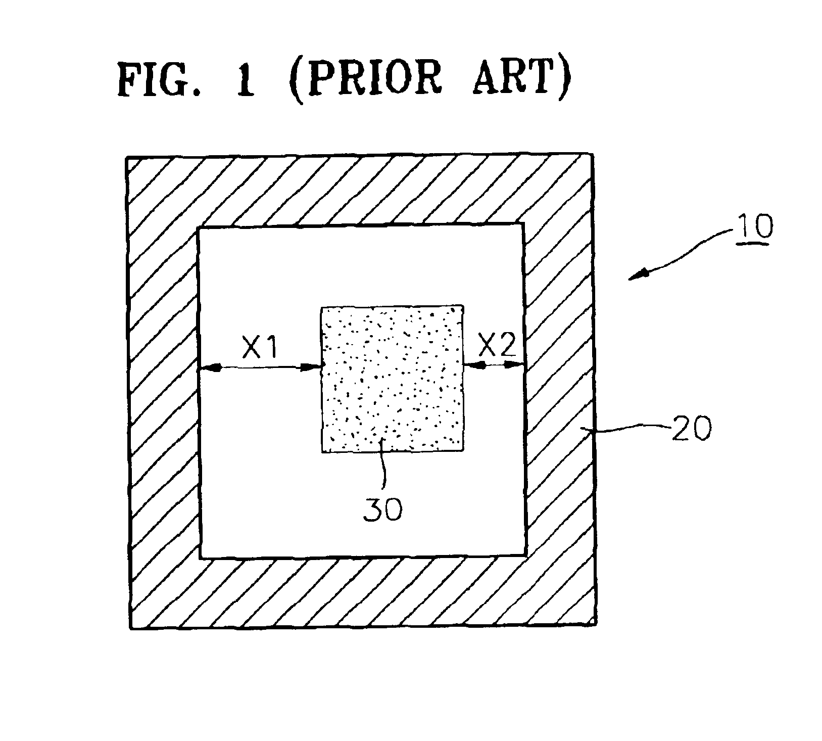
[0037]The present invention now will be described more fully with reference to the accompanying drawings, in which preferred embodiments of the invention are shown. This invention may, however, be embodied in many different forms and should not be construed as being limited to the embodiments set forth herein; rather, these embodiments are provided so that this disclosure will be thorough and complete, and will fully convey the concept of the invention to those skilled in the art.

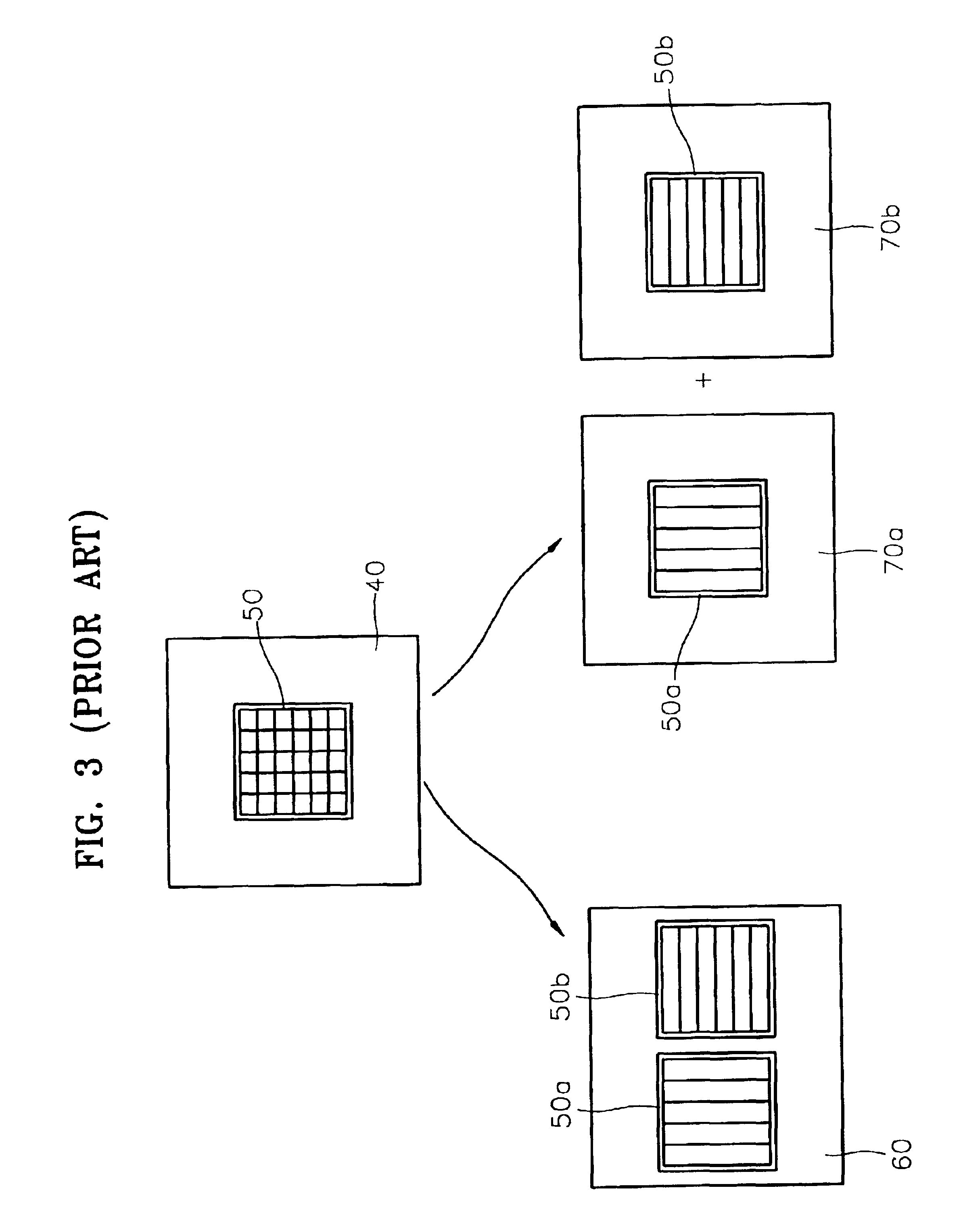
[0038]Unlike the conventional methods discussed above, the methods and systems of the present invention optimize algorithms for the exposure system so that the exposure system independently corrects overlays according to each sub-layout or sub-image. Therefore, the present invention is suitable for a multi-exposure process.

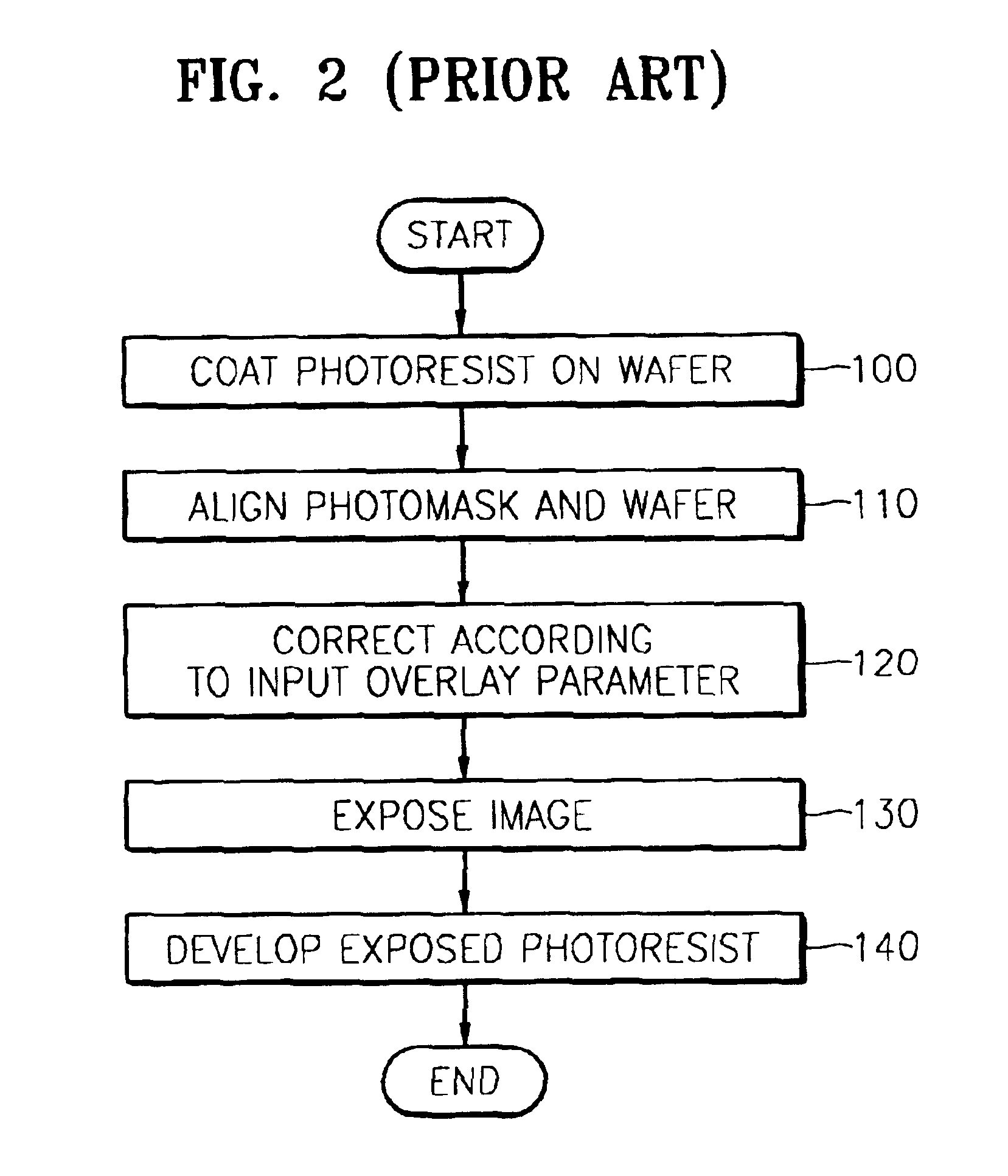
[0039]FIG. 7 is a flowchart of a multi-exposure lithography process according to an embodiment of the present invention. More specifically, FIG. 7 illustrates a method for performing an o...


PUM


Abstract

Multi-exposure lithography methods and systems that provide improved overlay accuracy. In one aspect of the invention, a method for multi-exposure lithography comprises determining overlay parameters corresponding to each of a plurality of sub-layouts, inputting the overlay parameters into an exposure system, exposing each sub-layout to photoresist on a wafer by using the exposure system, wherein prior to the exposure process for a given sub-layout, a correction process is performed for the sub-layout using a corresponding overlay parameter to correct an overlay of the sub-layout, and developing the exposed photoresist after exposing all of the sub-layouts.

Description

CROSS-REFERENCE TO RELATED APPLICATION[0001]This application claims priority to Korean Patent Application No. 02-16820 filed Mar. 27, 2002, which is incorporated herein by reference.BACKGROUND OF THE INVENTION[0002]1. Field of the Invention[0003]The present invention, generally, relates to a lithography process for semiconductor fabrication. More particularly, the present invention relates to multi-exposure lithography methods and systems that provide improved overlay accuracy.[0004]2. Description of Related Art[0005]To perform a lithography process for manufacturing semiconductor devices having a stack structure, the overlay between a preformed lower layer and an upper layer must be checked. As semiconductor devices become highly integrated and reduced in size, the accuracy of the overlay between the lower layers and the upper layers becomes increasingly more important to improve the reliability and yield of the semiconductor devices.[0006]Generally, the overlay is typically checke...

Claims


Application Information

Patent Timeline
IPC IPC(8): G03F7/20G03F9/00H01L21/027
CPCG03F7/70433G03F7/70466G03F7/70633H01L21/027
Inventor PARK, JOON-SOOPARK, CHANG-MIN
Owner SAMSUNG ELECTRONICS CO LTD
Why Eureka
Try Eureka