Mounting method for optical device and optical head equipment

a technology of optical head and mounting method, which is applied in the direction of optical beam source, semiconductor laser, instruments, etc., to achieve the effect of reducing the size and thickness of the optical head devi

Inactive Publication Date: 2005-11-15
NICHIA CORP
View PDF10 Cites 21 Cited by
  • Summary
  • Abstract
  • Description
  • Claims
  • Application Information

AI Technical Summary

Benefits of technology

[0100]According to this invention, face down mounting of a blue LD chip comprising a gallium nitride series compound semiconductor and having a step on the mounting surface can be realized. Accordingly, it is possible to provide an optical disk apparatus for recording and reproducing use in super DVD, DVD and CD by multi-wavelength integrated module having an optical source of multiple wavelengths including a blue LD.
[0101]The mounting method according to this invention allows an optical device having a step disposed on a mounting surface to be favorably mounted on a desired mounting substrate.
[0102]Further, the optical head device according to this invention is capable of decreasing the number of components, thereby reducing the size and thickness of the optical head device extremely usefully.

Problems solved by technology

When mounting is conducted by face down bonding, the following problems are present.

Method used


Image

  • Mounting method for optical device and optical head equipment
  • Mounting method for optical device and optical head equipment
  • Mounting method for optical device and optical head equipment

Examples


Embodiment Construction

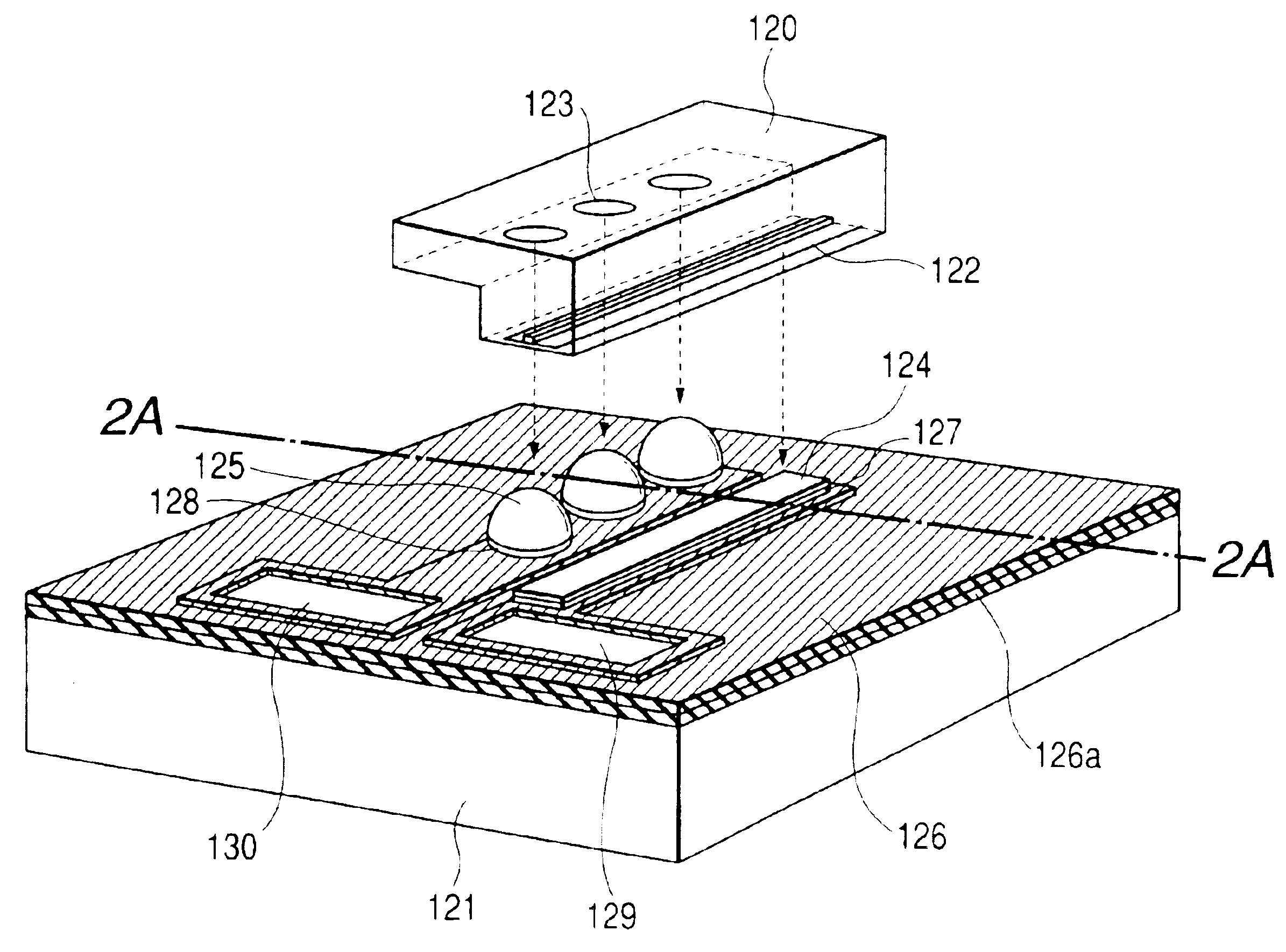
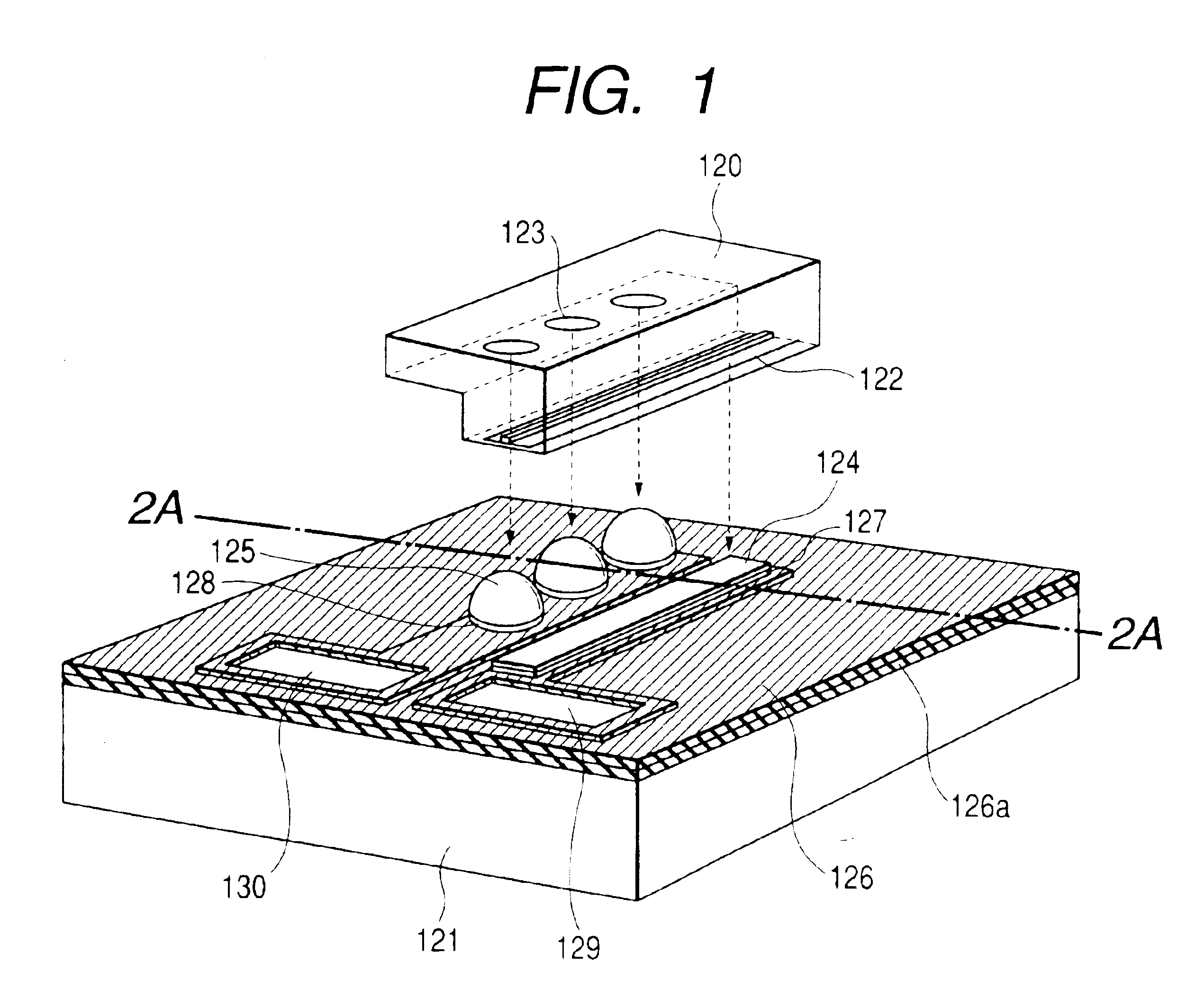
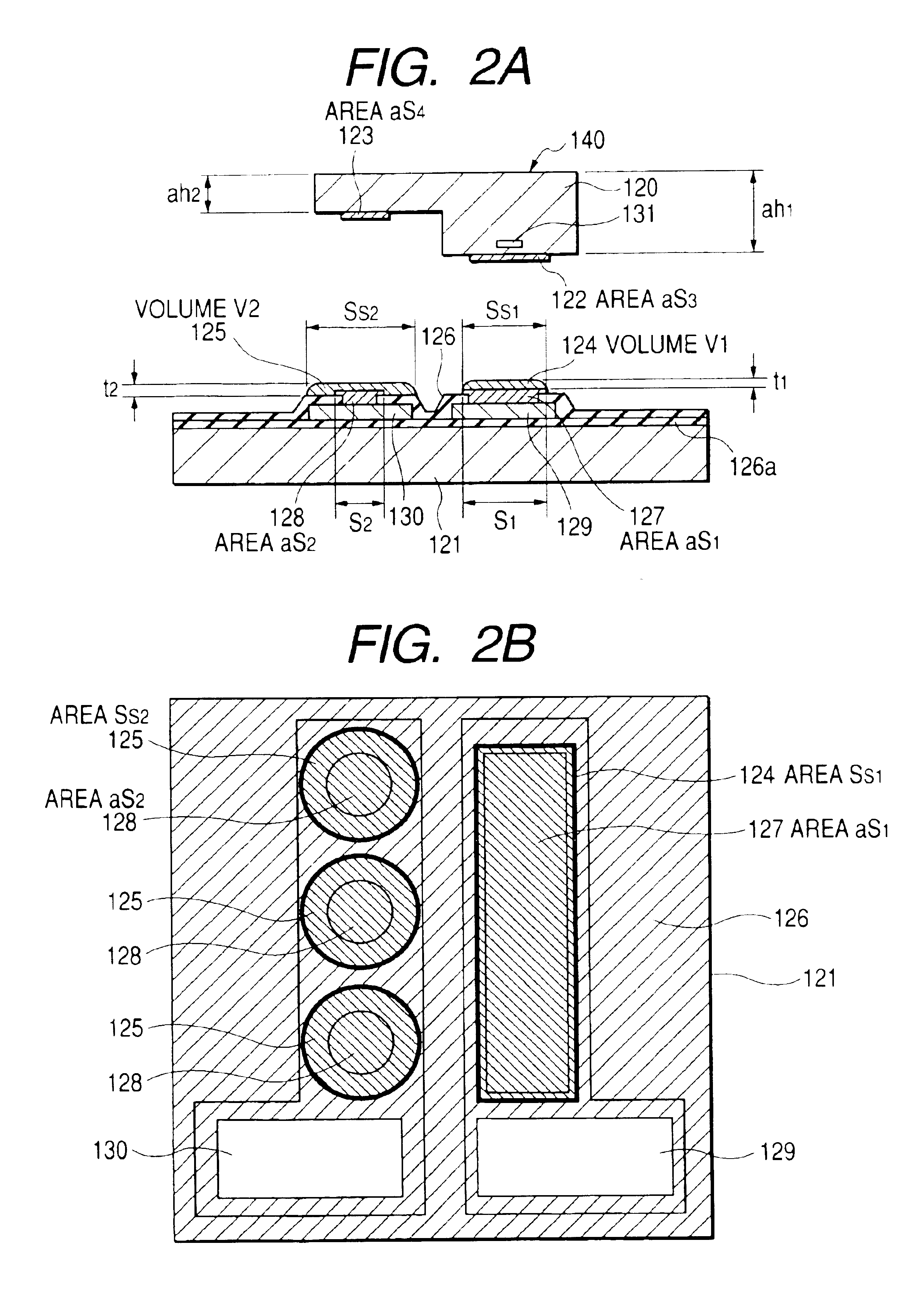
[0058]FIG. 1 is a perspective view showing an embodiment of a mounting structure according to this invention. An optical device 120 is opposed to an optical element mounting substrate 121. The optical device 120 has a step at a surface opposing to the substrate 121 for optical element mounting. A P-electrode 122 and an N-electrode 123 of the optical device are disposed on the surface at a first level and the surface at a second level, respectively, which form the step. A typical example of the optical device is, for example, a blue semiconductor laser (blue Laser Diode: hereinafter simply referred to as blue LD). Generally, in view of the restriction of the device manufacturing method, the blue LD has a structure in which the N-electrode is formed at a position lower by about 3 μm compared with the P-electrode having an active layer that emits light.

[0059]FIG. 1 shows a mounting structure in a case of mounting the blue LD 120 by face down bonding with an aim of improving the charact...


PUM

PropertyMeasurementUnit
wavelengthaaaaaaaaaa

Abstract

A method of mounting an optical device having a step on the surface opposing to a mounting substrate favorably by face-down bonding which enables a decrease in the number of components or integrate additional components on one identical substrate and, accordingly, is useful for reducing the size and the thickness of an optical head using a light source, the method includes the step of making the volume of a solder pattern to the area ratio of each electrode different for every wiring electrode portions upon mounting the electrodes on the substrate for mounting the optical device, in which the optical device having the step can be mounted favorably to the substrate by the control for the height of solder upon melting.

Description

BACKGROUND OF THE INVENTION[0001]1. Field of the Invention[0002]The present invention relates to a method of mounting an optical device having a step on an outer profile of an element on a substrate by face down bonding and a mounting structure. The present invention more particularly relates to an optical integrated module device mounting an optical device by the mounting method and the mounting structure described above and an optical device such as an integrated optical head device using the same.[0003]2. Related Art[0004]A nitride semiconductor laser device capable of oscillating a blue laser light at a wavelength of about 410 nm has the following constitution. That is, a nitride semiconductor material comprising InGaN as an active layer and AlGaN as a clad layer are crystallographically grown on a gallium nitride (GaN) substrate by a crystal growing method[0005]When such a blue semiconductor laser is put to practical use, the recording capacity of existent DVD apparatus using r...

Claims


Application Information

Patent Timeline
Patent Type & Authority Patents(United States)
IPC IPC(8): G11B7/22G11B7/125G11B7/12G11B7/00H05K3/34G11B7/09G11B7/13H01S5/022H01S5/323
CPCG11B7/1205G11B7/127G11B7/22G11B2007/0006H05K3/341H05K3/3436G11B7/123H01S5/02
Inventor TOKUDA, MASAHIDETATSUNO, KIMIOSANO, HIROHISASHIMANO, TAKESHIKIMURA, SHIGEHARU
Owner NICHIA CORP
Why Eureka
Try Eureka