Process for manufacturing a substrate with embedded capacitor

Active Publication Date: 2005-11-22
ADVANCED SEMICON ENG INC
View PDF7 Cites 33 Cited by
  • Summary
  • Abstract
  • Description
  • Claims
  • Application Information

AI Technical Summary

Benefits of technology

[0006]The secondary object of the present invention is to provide a process for manufacturing a substrate with an embedded capacitor. A dielectric layer is formed on the substrate base by build-up coating. A hole is formed in the dielectric layer for filling a medium material. The medium material can be filled into the hole of the dielectric layer to solve the problems of overflow or insufficiency of the medium material caused by the conventional laminated method.
[

Problems solved by technology

In accordance with this known manufacturing method, the upper/lower metal layers on the dielectric layer cannot directly provide the upper/lower electrode pads of the embedded capacitors due to the holes.
Moreover it is difficult to manufacture the plating layer covering the medium material to be flat, that is because that the filling quantity of the medium material in each hole cannot be control

Method used


Image

  • Process for manufacturing a substrate with embedded capacitor
  • Process for manufacturing a substrate with embedded capacitor
  • Process for manufacturing a substrate with embedded capacitor

Examples


Embodiment Construction

[0013]Referring to the drawings attached, the present invention will be described by means of the embodiments below.

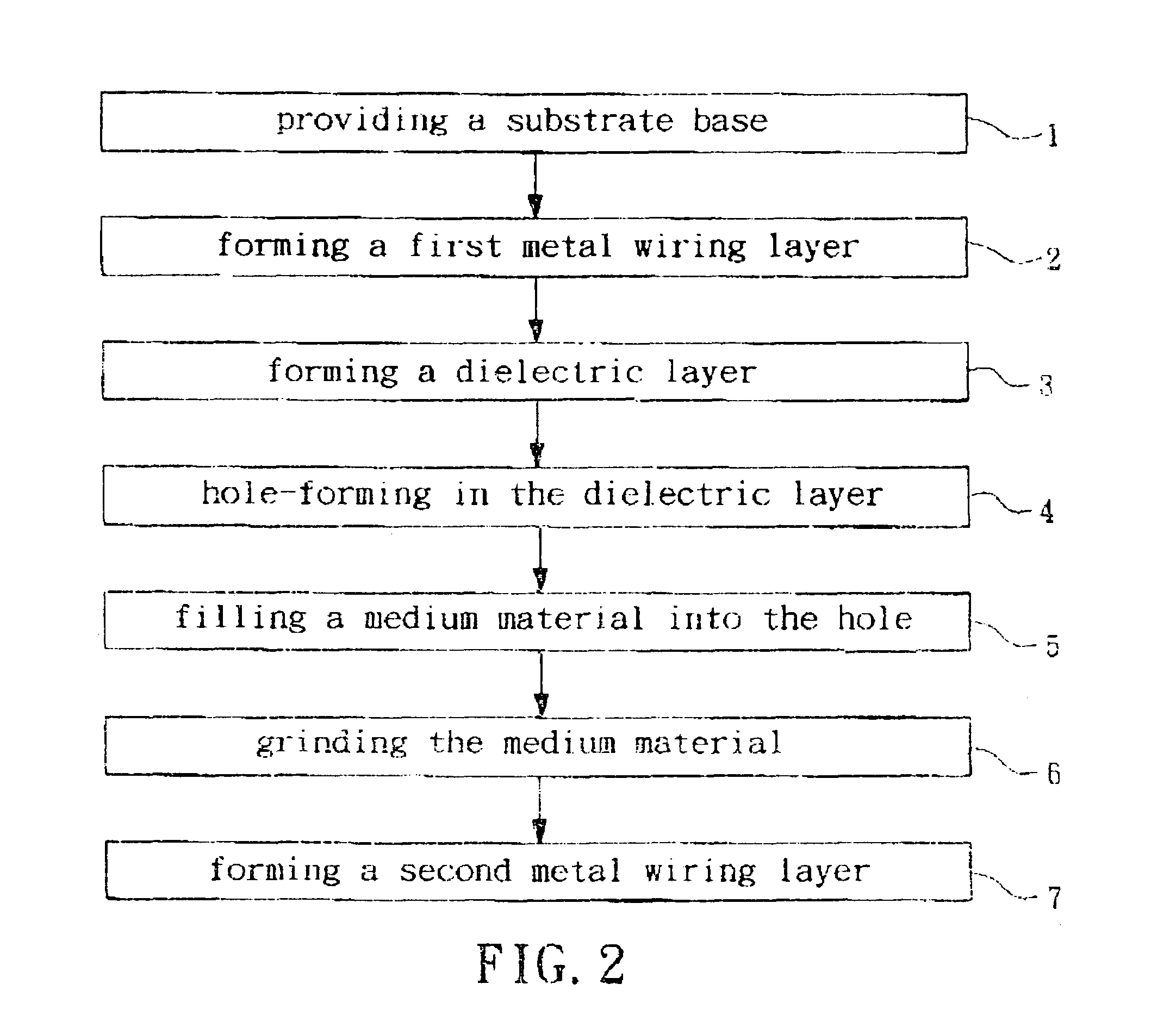
[0014]Referring to FIG. 2, the process for manufacturing a substrate with an embedded capacitor in accordance with the present invention mainly comprises: the step 1 of “providing a substrate base”, the step 2 of “forming a first metal wiring layer”, the step 3 of “forming a dielectric layer by build-up coating”, the step 4 of “hole-forming in the dielectric layer”, the step 5 of “filling a medium material into the hole”, the step 6 of “grinding the medium material” and the step 7“forming a second metal wiring layer”.

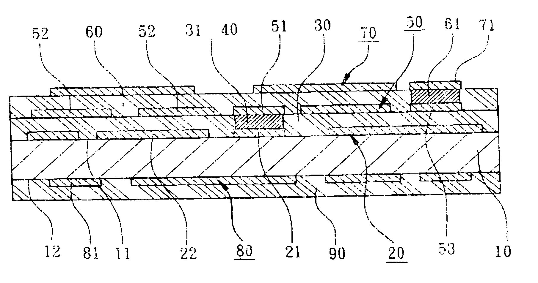
[0015]Referring to FIG. 3A, in the step 1, a substrate base 10 is provided. The substrate base 10 has an upper surface 11 and a lower surface 12, wherein the substrate base 10 may be a glass fiber reinforced resin layer, a single-layer PCB, multi-layer PCB with circuit pattern or a core. Referring to FIG. 3B, in the forming step 2, a first metal wiring lay...


PUM


Abstract

A process for manufacturing a substrate with an embedded capacitor is disclosed. A first metal wiring layer including a lower electrode pad is formed on a substrate base. A dielectric layer is formed a on the substrate base by build-up coating. A hole is formed in the dielectric layer to expose the lower electrode pad, then a medium material is filled into the hole. The medium material is ground to have a ground surface coplanar to the dielectric layer. A second metal wiring layer including an upper electrode pad is formed on dielectric layer, the upper electrode pad covers the ground surface of the medium material and is parallel to the lower electrode pad so as to form an embedded capacitor.

Description

FIELD OF THE INVENTION[0001]The present invention relates to a method for manufacturing a substrate for IC, particularly to a process for manufacturing a substrate with an embedded capacitor.BACKGROUND OF THE INVENTION[0002]It is understood that conventional passive components, such as capacitors, resistors or inductors, are separately manufactured to be individual passive components for mounting on a substrate. In order to answer the strict requirements including electrical conductivity and elements simplification in the semiconductor packaging field, the passive components, especially capacitor, should be integrated into a printed circuit board (IC substrate).[0003]A method for manufacturing a multi-layer substrate with embedded capacitor is disclosed in R.O.C. Taiwan Patent No. 440,993. A plurality of through holes are formed in a dielectric layer and pass through upper / lower metal layers. The lower metal layer is used as a ground layer without traces. A medium material is filled...

Claims


Application Information

Patent Timeline
IPC IPC(8): H01L21/48H01L21/02H05K1/16H05K3/00H05K3/46
CPCH01L21/4857H05K1/162H05K3/0023H05K3/0035H05K3/4644H05K2201/0187H05K2203/1461
Inventor DING, YI-CHUAN
Owner ADVANCED SEMICON ENG INC
Why Eureka
Try Eureka