

Method for the electron-microscopic observation of a semiconductor arrangement and apparatus therefor
a semiconductor and electron microscopic technology, applied in semiconductor/solid-state device testing/measurement, instruments, therapy, etc., can solve the problems of difficult to image structures with a high aspect ratio significant number of such secondary electrons cannot enter the objective of the microscope, and the depth of the structure cannot be satisfactorily imaged by means of sem, etc., to achieve the effect of increasing flexibility and high aspect ratio
- Summary
- Abstract
- Description
- Claims
- Application Information
AI Technical Summary
Benefits of technology
Problems solved by technology
Method used
Image

Examples
Embodiment Construction
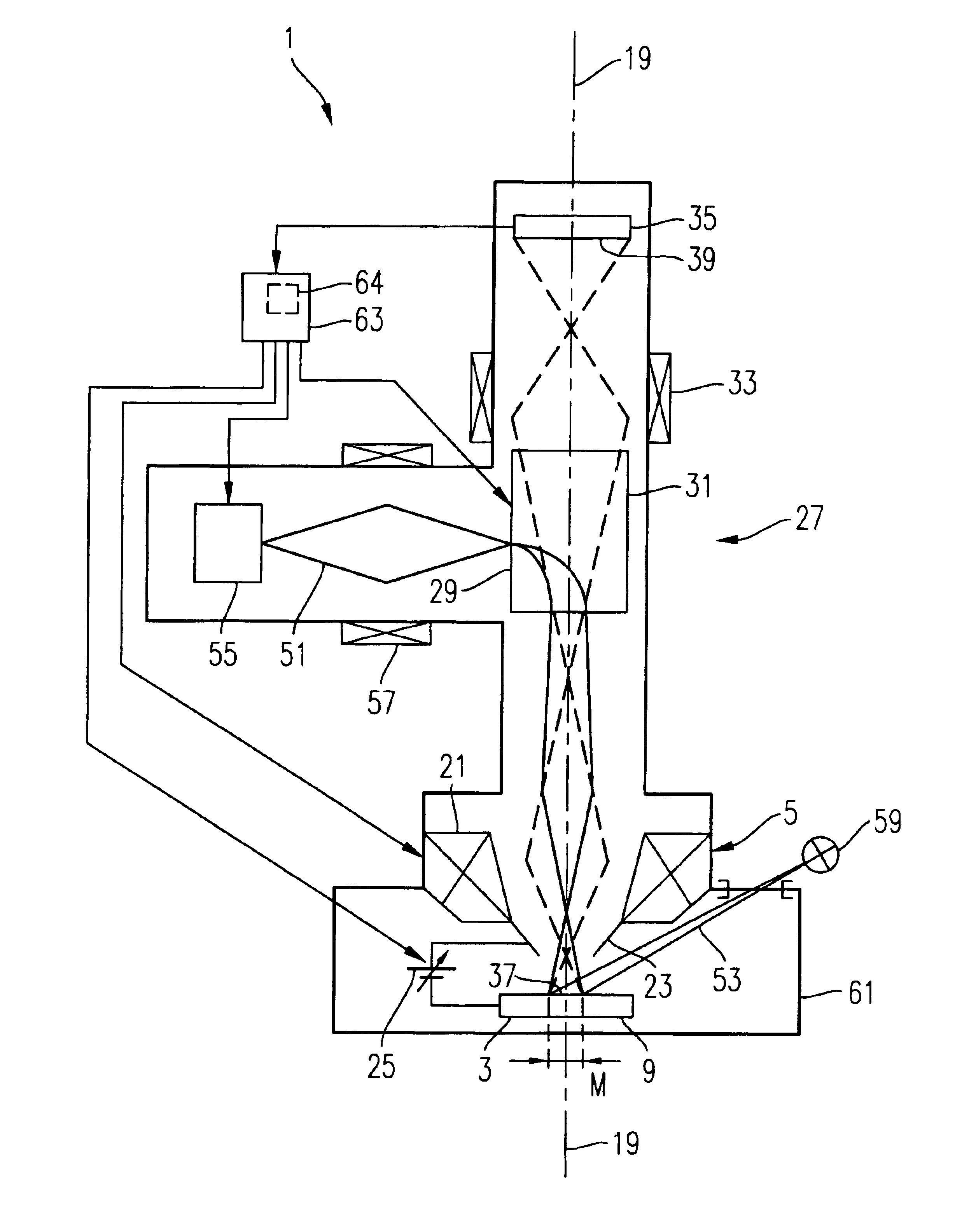
[0058]FIG. 1 schematically shows an electron microscope 1 which is suitable for implementing the method according to the invention. The electron microscope 1 serves to examine a semiconductor structure 3 which is positioned as object to be examined in front of an objective system 5 of the electron microscope 1.
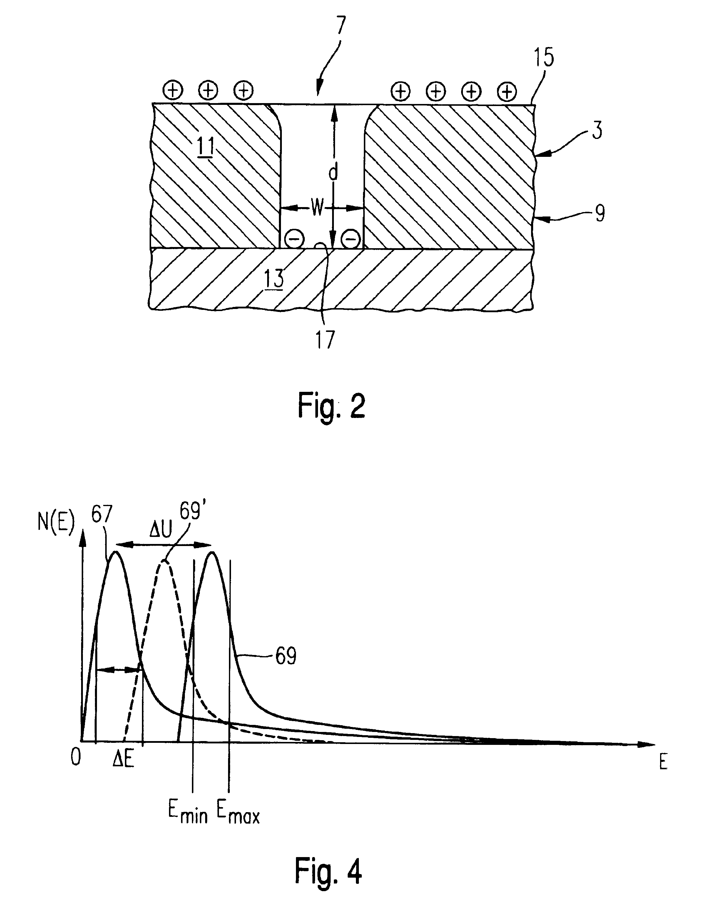
[0059]The semiconductor arrangement 3 constitutes, for example, a part of a semiconductor wafer or the like and has a topology comprising structures with a high aspect ratio, as it is shown schematically in FIG. 2 with reference to a recess 7. The structure 3 shown in FIG. 2 forms part of a semiconductor wafer 9 and comprises a layer 11 of SiO2 of a thickness d of, for example, 2.5 μm which is deposited on a layer 13 of a metal, such as copper, for example. The SiO2 layer 11 has an upper surface 15 which faces towards the objective system 5 of the microscope 1. The recess 7 is formed in the SiO2 layer 11 and extends from the surface 15 through the SiO2 layer 11 as through hole...
PUM
| Property | Measurement | Unit |
|---|---|---|
| aspect ratio | aaaaa | aaaaa |
| aspect ratio | aaaaa | aaaaa |
| aspect ratio | aaaaa | aaaaa |
Abstract
Description
Claims
Application Information