Microfluidic array devices and methods of manufacturing and uses thereof

Inactive Publication Date: 2005-11-29
PHOENIX S&T
View PDF24 Cites 28 Cited by
  • Summary
  • Abstract
  • Description
  • Claims
  • Application Information

AI Technical Summary

Benefits of technology

[0014]In another aspect of the present application, the microfluidic nozzle array device is formed by an injection molding process that permits the microfluidic nozzle array device to have the above dimensions. A mold is first fabricated with the mold being a negative impression of the channel architecture and nozzle array that are formed as part of the microfluidic nozzle array device. Preferably, the mold is made of a metal material and with at least some portions of the mold being polished to a high degree of finish, i.e., a mirror finish. More spe

Problems solved by technology

In the absence of using microfluidic devices, the above processes and others are carried out in a manner that is very time intensive and thus, costly.
For example, large-scale protein profiling is commonly carried out laboriously but pervasively in the biotechnological and pharmaceutical industries.
While the stacking of multiple layers of planar substrates to form a microfluidic structure having layered microfluidic channels is possible in terms of its fabrication, the prevailing detection technology (optically based detection technology) limits the practicality of fabricating such a structure since parallel operation of multiple layers of the planar substrates containing multiple microfluidic separation channels is not practical due to each microfluidic separation channel requiring its own light source and detector.
This approach is laborious and is impractical for high throughput operations where many such holes have to be drilled sequentially into the substrates.
However, the use of silicon wafers as the substrates greatly limits the ability to individually activate each nozzle because of the potential of dielectric break

Method used


Image

  • Microfluidic array devices and methods of manufacturing and uses thereof
  • Microfluidic array devices and methods of manufacturing and uses thereof
  • Microfluidic array devices and methods of manufacturing and uses thereof

Examples


Example

EXAMPLE 1

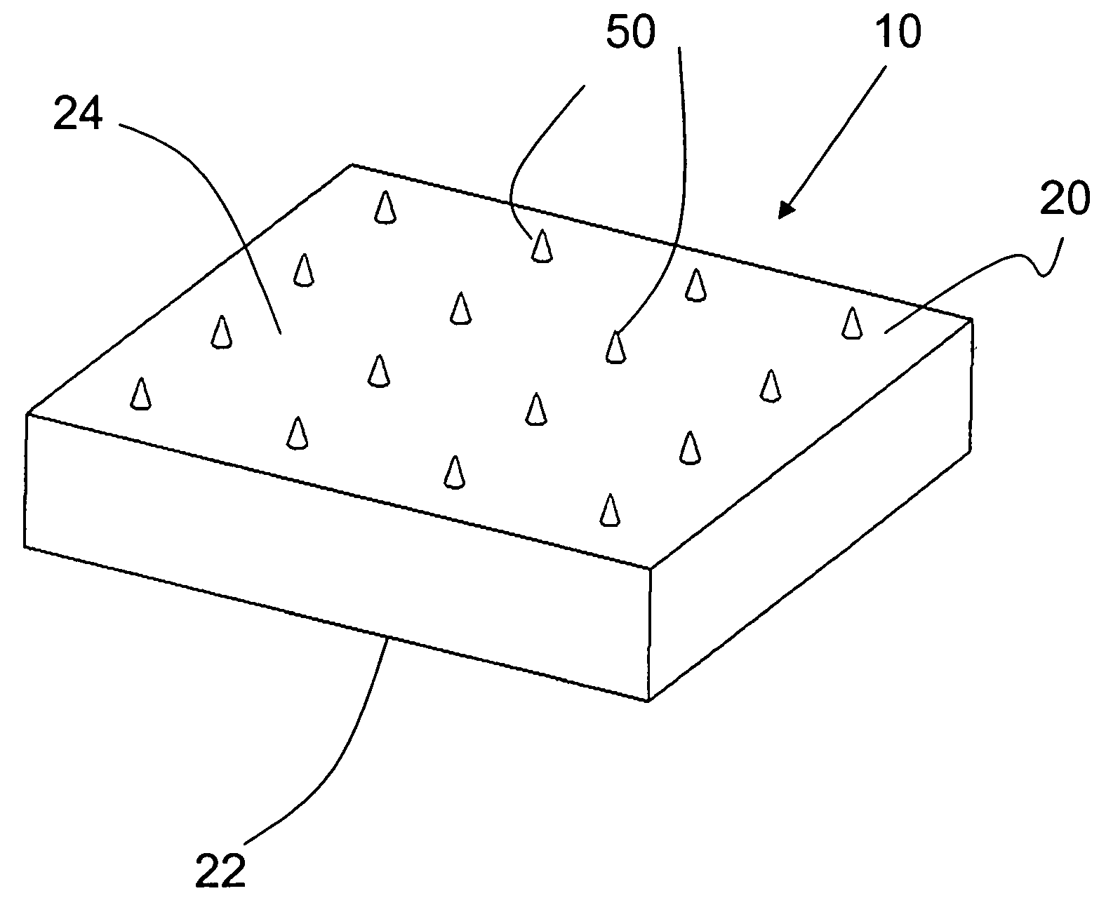
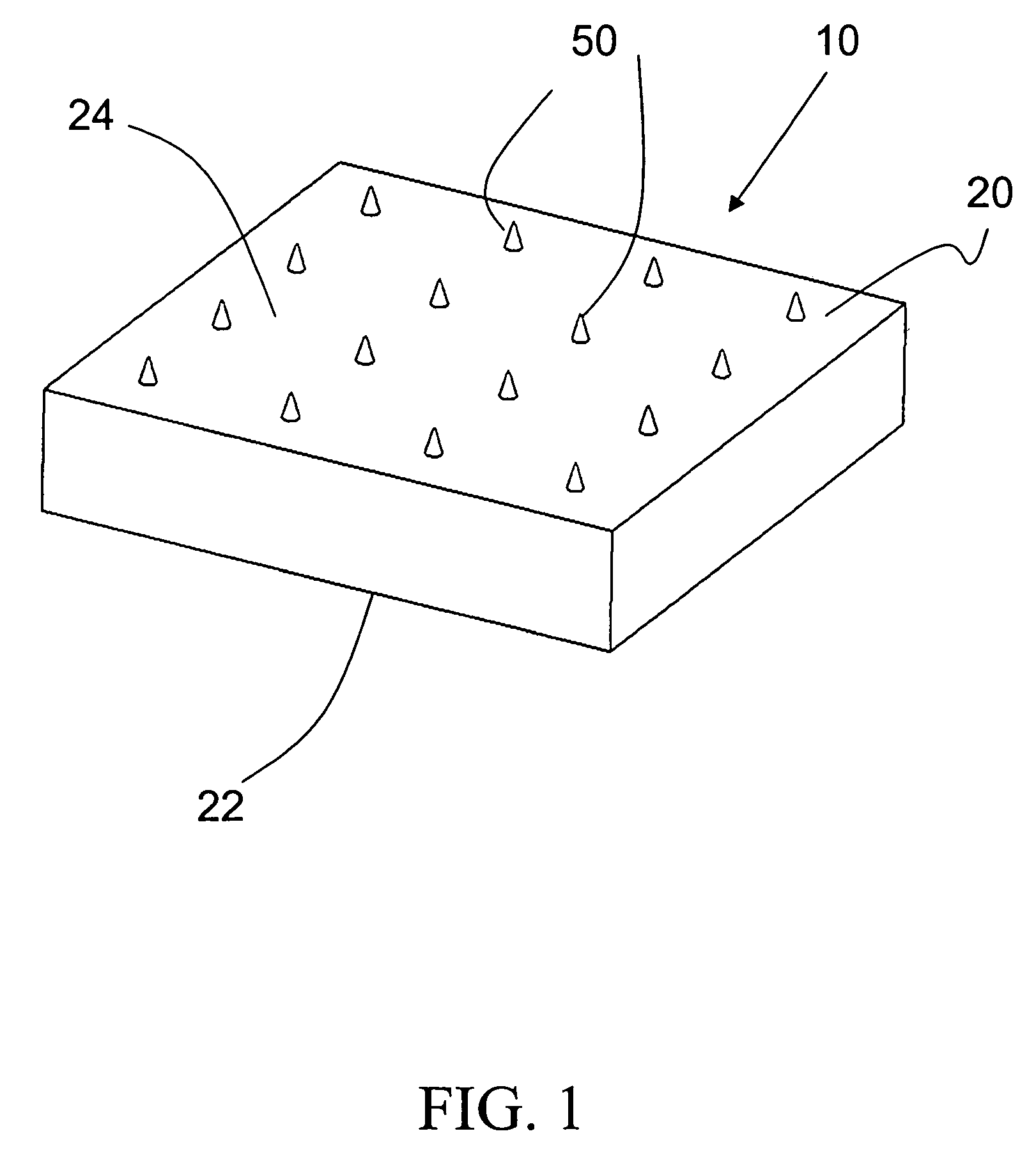
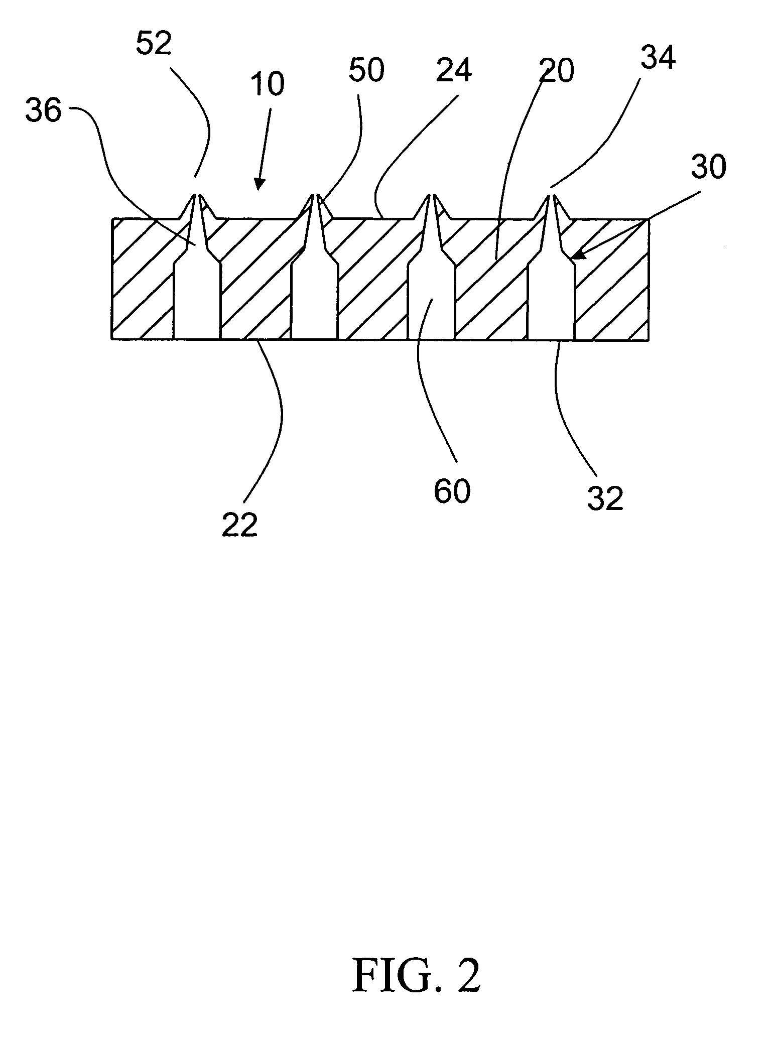
[0095]A polymeric microfluidic nozzle array device is fabricated using the technology disclosed herein is by first providing a mold designed for an injection mold process. The mold is formed of a metal and a conical surface of the mold that defines the nozzle portion of the microfluidic device is polished with a diamond paste to form a highly polished surface. More specifically, the conical surface is polished with 1 micron diamond particles to provide a close to mirror finish for the nozzle that is formed as part of the microfluidic device. The microfluidic device is fabricated by injecting polybutyl terephthalate (PBT) into the closed mold and then curing the formed structure and then ultimately removing the molded microfluidic nozzle array device from the mold. The microfluidic nozzle array device is formed to have nozzles that have an average outside diameter of about 60 microns and an average inside diameter of the tip (i.e., the diameter of the nozzle opening) being l...

Example

EXAMPLE 2

[0098]A polymeric microfluidic nozzle array device is fabricated using the technology disclosed herein by first providing a mold designed for an injection mold process. The mold is formed of a metal and a conical surface of the mold that defines the nozzle portion of the microfluidic device is polished with a diamond paste to form a highly polished surface. More specifically, the conical surface is polished with 1 micron diamond particles to provide a close to mirror finish for the nozzle that is formed as part of the microfluidic device. The microfluidic device is fabricated by injecting polybutyl terephthalate (PBT) into the closed mold and then curing the formed structure and then ultimately removing the molded microfluidic nozzle array device from the mold. The microfluidic nozzle array device is formed to have nozzles that have an average outside diameter of about 60 microns and an average inside diameter of the tips (i.e., the diameter of the nozzle opening) being les...

Example

EXAMPLE 3

[0100]A polymeric microfluidic nozzle array device is fabricated using the technology disclosed herein by first providing a mold designed for an injection mold process. The mold is formed of a metal and a conical surface of the mold that defines the nozzle portion of the microfluidic device is polished with a diamond paste to form a highly polished surface. More specifically, the conical surface is polished with 1 micron diamond particles to provide a close to mirror finish for the nozzle that is formed as part of the microfluidic device. The microfluidic device is fabricated by injecting polybutyl terephthalate (PBT) into the closed mold and then curing the formed structure and then ultimately removing the molded microfluidic nozzle array device from the mold. The microfluidic nozzle array device is formed to have nozzles that have an average outside diameter of about 60 microns and an average inside diameter of the tips (i.e., the diameter of the nozzle opening) being les...


PUM

PropertyMeasurementUnit
Diameteraaaaaaaaaa
Diameteraaaaaaaaaa
Diameteraaaaaaaaaa

Abstract

Microfluidic nozzle array devices are provided with the body of each device having at least one nozzle extending outwardly from one surface of the body. Each nozzle includes a tip opening having a diameter of equal to or less than about 100 μm, preferably 50 μm, and more preferably 20 μm and an outer diameter of nozzle is equal to or less than about 150 μm, preferably 100 μm, and more preferably 50 μm. The microfluidic nozzle array devices are fabricated using an injection molding process and find particular utility in a wide range of applications, including but not limited to nanospray/electrospray applications, mass spectrometer applications, optical spectrometry applications, spotting applications (i.e., DNA or protein array), etc.

Description

CROSS-REFERENCE TO RELATED APPLICATIONS[0001]This application is a divisional application of U.S. patent application Ser. No. 10 / 174,343, filed Jun. 17, 2002 which claims the benefit of U.S. patent application Ser. No. 60 / 341,069, filed Dec. 19, 2001, which are hereby incorporated by reference in their entirety.TECHNICAL FIELD[0002]The present invention relates to microfluidic devices, and more particularly, to microfluidic array devices that can be used to deliver one or more samples through one or more nozzles that are formed as part of the microfluidic array device. Exemplary manufacturing methods for fabrication of the microfluidic array devices are also disclosed as well as exemplary uses for the microfluidic array devices. For example, the microfluidic array device is suitable for operations designed for lab-on-a-chip functions including analysis of components in the sample fluid by means of optical spectrometry, mass spectrometry, etc.BACKGROUND[0003]There has been a growing ...

Claims


Application Information

Patent Timeline
IPC IPC(8): B01L3/00B01L3/02B01L9/00B81B1/00C40B60/14G01N27/447G01N30/28G01N30/60G01N35/10H01J49/04
CPCH01J49/0431B01L3/0268B01L3/5027B01L9/527G01N27/44782G01N27/44791B01J2219/0036B01L3/0241B01L3/5025B01L3/502707B01L2200/021B01L2200/027B01L2400/027B01L2400/0481C40B60/14G01N30/6026G01N30/6095G01N35/1074G01N2030/285G01N2035/1039B33Y80/00
Inventor STAATS, SAU LAN TANG
Owner PHOENIX S&T
Why Eureka
Try Eureka