
Display panel

a display panel and panel technology, applied in the field of display panels, can solve the problems of low product yield rate, and achieve the effect of improving the yield rate of the display panel, effective and precisely detected

Active Publication Date: 2017-05-02
TCL CHINA STAR OPTOELECTRONICS TECH CO LTD
View PDF3 Cites 2 Cited by
  • Summary
  • Abstract
  • Description
  • Claims
  • Application Information

AI Technical Summary

Benefits of technology

[0008]An object of the present invention is to provide a display panel where a short-circuit condition occurring in the display panel can be effectively and precisely detected so as to improve the yield rate of the display panel.
[0030]Compared with the conventional technologies, in the display panel of the present invention, the short-circuit condition can be detected during the TFT manufacturing process of the display panel, therefore it helps to increase the efficiency and accuracy of detecting the short circuit condition in the display panel and also helps to improve the yield rate of the display panel and reduce the manufacturing cost of the display panel.

Problems solved by technology

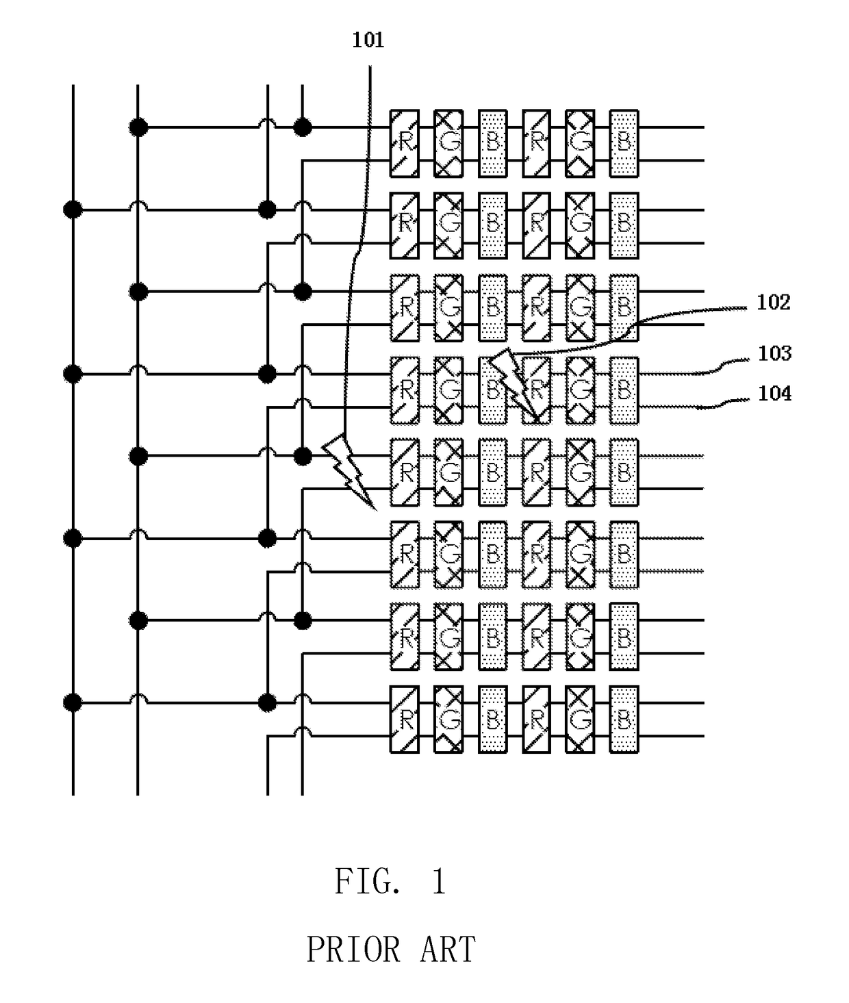
Thus, if there is a short-circuit condition occurs between a charging scanning line 103 and a charge-sharing scanning line 104 of the same pixel row, such as the first short-circuit position 101 or the second short-circuit position 102 shown in FIG. 1, then the foregoing inspection method of using the shorting bar to connect all of the odd-numbered lines or all of the even-numbered lines cannot detect this short-circuit condition during the TFT manufacturing process, thereby causing low product yield rate.

Method used


Image

  • Display panel
  • Display panel
  • Display panel

Examples


Embodiment Construction

[0035]The following description of each embodiment is referring to the accompanying drawings so as to illustrate practicable specific embodiments in accordance with the present invention.

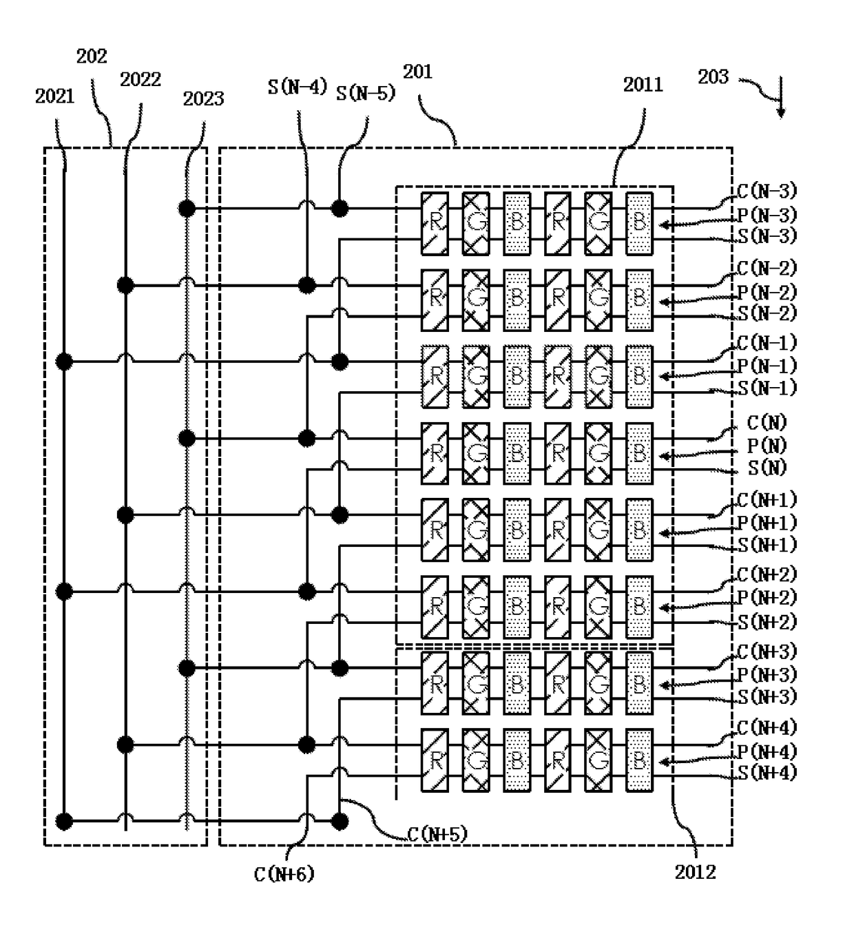
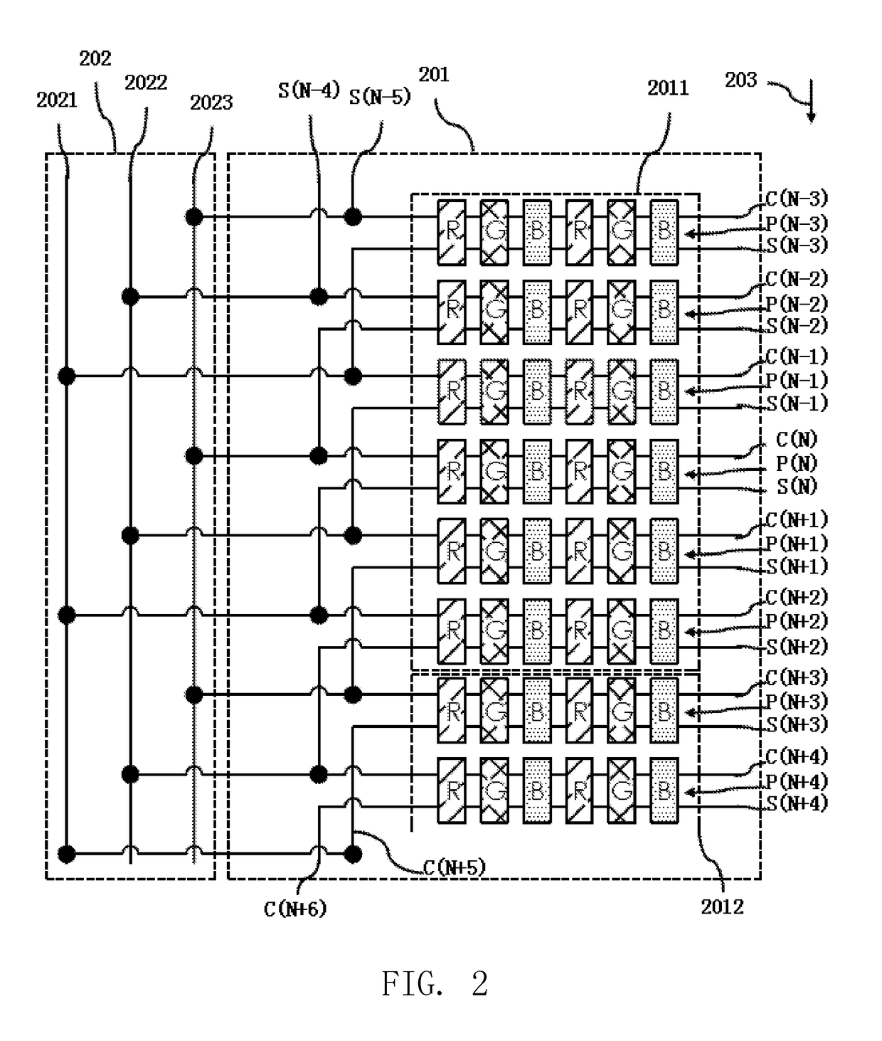
[0036]Please refer to FIG. 2, which is a schematic diagram of a display panel according to a first embodiment of the present invention.

[0037]The display panel of the present embodiment may be an LCD (Liquid Crystal Display) panel, an OLED (Organic Light Emitting Diode) display panel or the like.

[0038]The display panel of the embodiment comprises an active area 201 and at least one non-active area 202. The at least one non-active area is disposed beside the active area 201. For example, there may be two non-active areas being arranged at two sides of the active area 201. The display panel is provided with a pixel array. The pixel array is disposed in the active area 201 and is formed by a plurality of pixels.

[0039]Specifically, the active area 201 is provided with at least two array units (2011, 2012...


PUM

PropertyMeasurementUnit
areaaaaaaaaaaa
charge-aaaaaaaaaa
chargeaaaaaaaaaa

Abstract

A display panel is disclosed and includes an active area and a non-active area. A first, a second, a third, a fourth, a fifth, and a sixth charging scanning lines and a first, a second, a third, a fourth, a fifth, and a sixth charge-sharing scanning lines of an array unit on the active area are connected to a first, a second, a third, a fourth, a fifth, and a sixth pixel row, respectively. A first, a second, and a third detection lines on the non-active area are connected to the active area.

Description

RELATED APPLICATIONS[0001]This application is a National Phase of PCT Patent Application No. PCT / CN2014 / 083859 having International filing date of Aug. 7, 2014, which claims the benefit of priority of Chinese Patent Application No. 201410308596.1 filed on Jun. 30, 2014. The contents of the above applications are all incorporated by reference as if fully set forth herein in their entirety.BACKGROUND OF THE INVENTION[0002]Field of the Invention[0003]The present invention relates to the field of display technology, and more particularly to a display panel.[0004]Description of the Related Art[0005]In a traditional circuit design of display panels, there are peripheral wires mounted around the pixel area for shorting-bar connection, wherein the odd-numbered and even-numbered scanning lines are guided to the peripheral wires, respectively, meaning that the odd-numbered / even-numbered scanning lines are connected together at the periphery of the display panel. Such design is to give differe...

Claims


Application Information

Patent Timeline
Patent Type & Authority Patents(United States)
IPC IPC(8): G02F1/1362H01L27/12G02F1/13H01L27/32G09G3/00
CPCH01L27/1244G02F1/1309G02F1/136259G09G3/006H01L27/3211G02F2001/136254G02F2001/136263G09G2300/0413G09G2300/0426H01L27/3276G02F1/136254G02F1/136263H10K59/35H10K59/131G02F1/1343G09G3/36G09G2300/0421G09G2310/0262G09G3/20G09G3/3225G09G3/3648G09G2300/0452
Inventor WANG, ZUIGUO, JINBO
Owner TCL CHINA STAR OPTOELECTRONICS TECH CO LTD
Learn More