Method of manufacturing semiconductor device and semiconductor device

a manufacturing method and semiconductor technology, applied in the direction of semiconductor devices, electrical appliances, transistors, etc., can solve the problems of large drop in threshold voltage, sub-threshold coefficient s becomes more pronounced, and the threshold voltage becomes more pronounced, so as to effectively inhibit the short channel

Inactive Publication Date: 2005-12-13
LAPIS SEMICON CO LTD
View PDF2 Cites 0 Cited by
  • Summary
  • Abstract
  • Description
  • Claims
  • Application Information

AI Technical Summary

Benefits of technology

[0014]It is an objective of the invention to provide a method of manufacturing a semiconductor device and a semiconductor device so as to effectively inhibit the short channel effect resulting from a reduction of the gate length attendant with miniaturization of the SOI-MOSFET.
[0015]To achieve this object, in a method of manufacturing a semiconductor device and a semiconductor device, impurity ions are implanted into the SOI layer so that a distribution of an impurity ion concentration in the SOI layer inhibits a reduction in a threshold voltage (Vth-rolloff) of the device.
[0016]According to the present invention, a reduction in a potential barrier can be effectively inhibited, which in turn can effectively inhibit the short channel effect resulting from a reduction in the gate length.

Problems solved by technology

However, as the gate length is reduced even further, the fall in the threshold voltage becomes more pronounced, until eventually small reductions in gate length result in large drops in the threshold voltage.
However, as the gate length is reduced even further, the rise in the sub-threshold coefficient S becomes more pronounced, until eventually small reductions in gate length result in large increases in the sub-threshold coefficient S. Also, the larger the sub-threshold coefficient S, the larger becomes an off-leak current.
As such, small reductions in gate length can result in large increases in the sub-threshold coefficient S and in the off-leak current.

Method used


Image

  • Method of manufacturing semiconductor device and semiconductor device
  • Method of manufacturing semiconductor device and semiconductor device
  • Method of manufacturing semiconductor device and semiconductor device

Examples


Embodiment Construction

[0040]Preferred embodiments of the present invention will hereinafter be described in detail with reference to the accompanying drawings. The drawings used for this description typically illustrate major characteristic parts in order that the present invention will be easily understood.

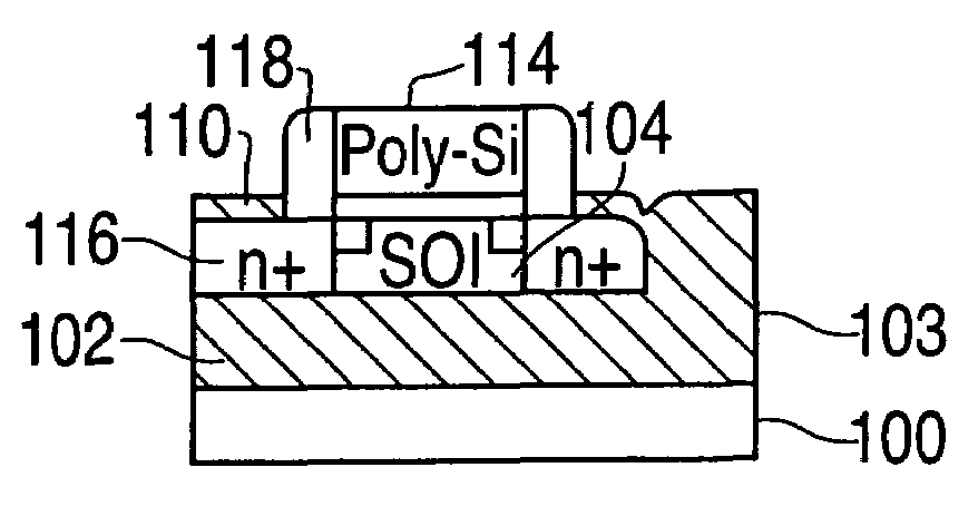
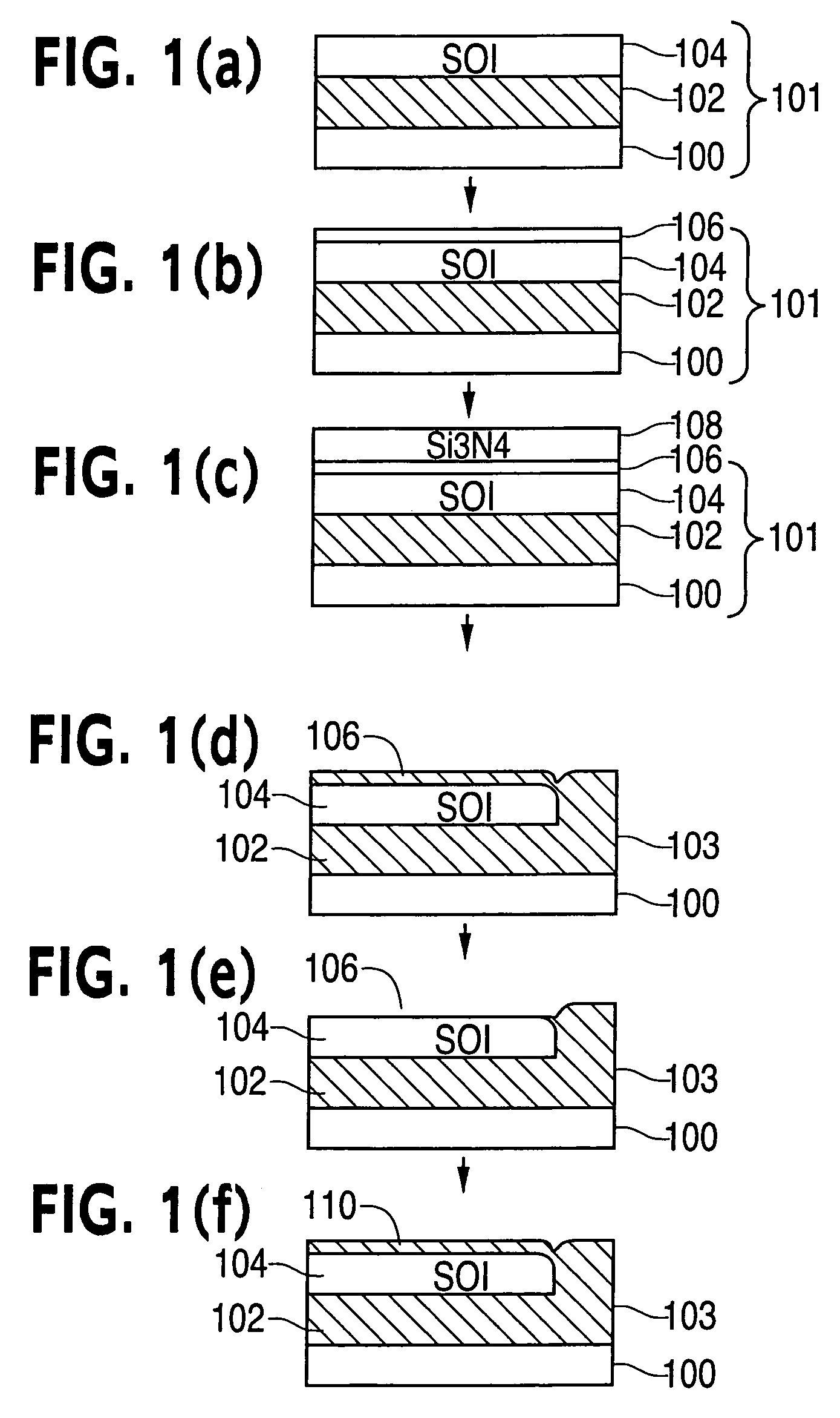
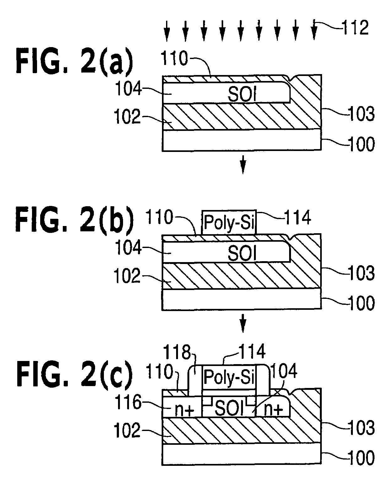
[0041]FIGS. 1(a) through 1(f) and FIGS. 2(a) through 2(c) are cross-sectional views for explaining a method of manufacturing a semiconductor device according to a first preferred embodiment of the present invention. An SOI substrate 101 is first prepared which includes a silicon substrate 100, an oxide film 102 and an SOI layer 104, as shown in FIG. 1(a). A pad oxide film 106 is formed on the SOI layer 104, as shown in FIG. 1(b), and then a nitride film (Si3N4) 108 is formed on the pad oxide film 106, as shown in FIG. 1(c). Then, an isolation film 103 is formed by a LOCOS method or an STI method, as shown in FIG. 1(d). Thereafter, the pad oxide film 106 is removed, as shown in FIG. 1(e), and then a th...


PUM


Abstract

Impurity ions are implanted into the silicon layer of an SOI substrate to achieve an ion concentration distribution which inhibits for a reduction in threshold voltage (Vth-rolloff) as a gate length is reduced. A reduction in potential barrier which runs from a drain region side is effectively inhibited to counter short channel effects resulting from a reduction in gate length attendant with miniaturization of SOI-MOSFETs.

Description

CROSS-REFERENCE TO RELATED APPLICATIONS[0001]This is a divisional of application Ser. No. 10 / 092,499, filed Mar. 8, 2002, now U.S. Pat. No. 6,825,074 which is incorporated herein by reference in its entirety.BACKGROUND OF THE INVENTION[0002]1. Field of the Invention[0003]The present invention relates to a method of manufacturing a MOSFET which is formed in a silicon on insulator (SOI) substrate, and more particularly to a method of implanting ions into a silicon layer of the SOI substrate to control a threshold voltage of the SOI-MOSFET. And, the present invention relates to a semiconductor device which is formed in the SOI substrate, and more particularly to a peak ion concentration of the silicon layer of the SOI-MOSFET.[0004]The present application claims priority under 35 U.S.C. §119 to Japanese Patent Application No. 2001-68895, filed Mar. 12, 2001, which is herein incorporated by reference in its entirely for all purposes.[0005]2. Description of the Related Art[0006]A conventi...

Claims


Application Information

Patent Timeline
Patent Type & Authority Patents(United States)
IPC IPC(8): H01L27/08H01L21/265H01L21/336H01L21/762H01L21/8238H01L27/092H01L29/786
CPCH01L21/76264H01L29/66772H01L29/78654H01L29/78696H01L21/76281
Inventor MIURA, NORIYUKI
Owner LAPIS SEMICON CO LTD
Why Eureka
Try Eureka