
Low power current input delta-sigma ADC using injection FET reference

Active Publication Date: 2005-12-20
RAYTHEON CO
View PDF5 Cites 97 Cited by
  • Summary
  • Abstract
  • Description
  • Claims
  • Application Information

AI Technical Summary

Benefits of technology

[0012]In another aspect of the invention is a readout circuit. The readout circuit includes an input node for receiving a photocurrent generated by a radiation detector. The photocurrent represents the analog signal to be converted by the readout circuit, and refers to any current signal output by the various types of radiation detectors. The circuit further includes an integrating capacitor having a first node coupled to the input node, and a comparator. A first comparator input is coupled to the first node of the integrating capacitor and a second comparator input is coupled to a first reference signal. The circuit further includ

Problems solved by technology

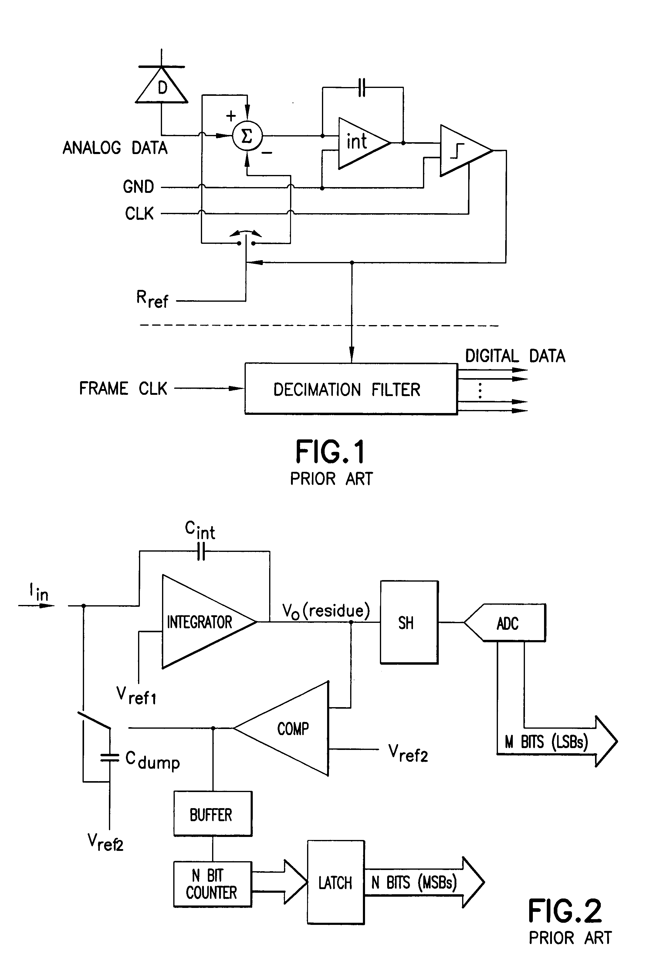
However, this design typically requires a large counter that must be present in each ADC.
Further, for a given frame time, the maximum signal to noise ratio (SNR) is constrained by the pixel area, clock frequency, and power limitations.
One difficulty with prior art designs is that they generally employ an amplifier that consumes too much power for use in a large imaging array, such as an array of infrared detectors.
Further, noise is captured at the end of every charge dump event but auxiliary ADC quantization noise is the largest noise contribution.
While the residue-readout ADC does not require 20-bits in the cell (unlike conventional ADCs), it requires the noted auxiliary ADC and provides poor power per pixel when used in an imaging array.
Performance is limited by pixel array constraints, and implementation details.
However, these implementations each require significant power to achieve the bandwidth for use in an imaging array.

Method used


Image

  • Low power current input delta-sigma ADC using injection FET reference
  • Low power current input delta-sigma ADC using injection FET reference
  • Low power current input delta-sigma ADC using injection FET reference

Examples


Embodiment Construction

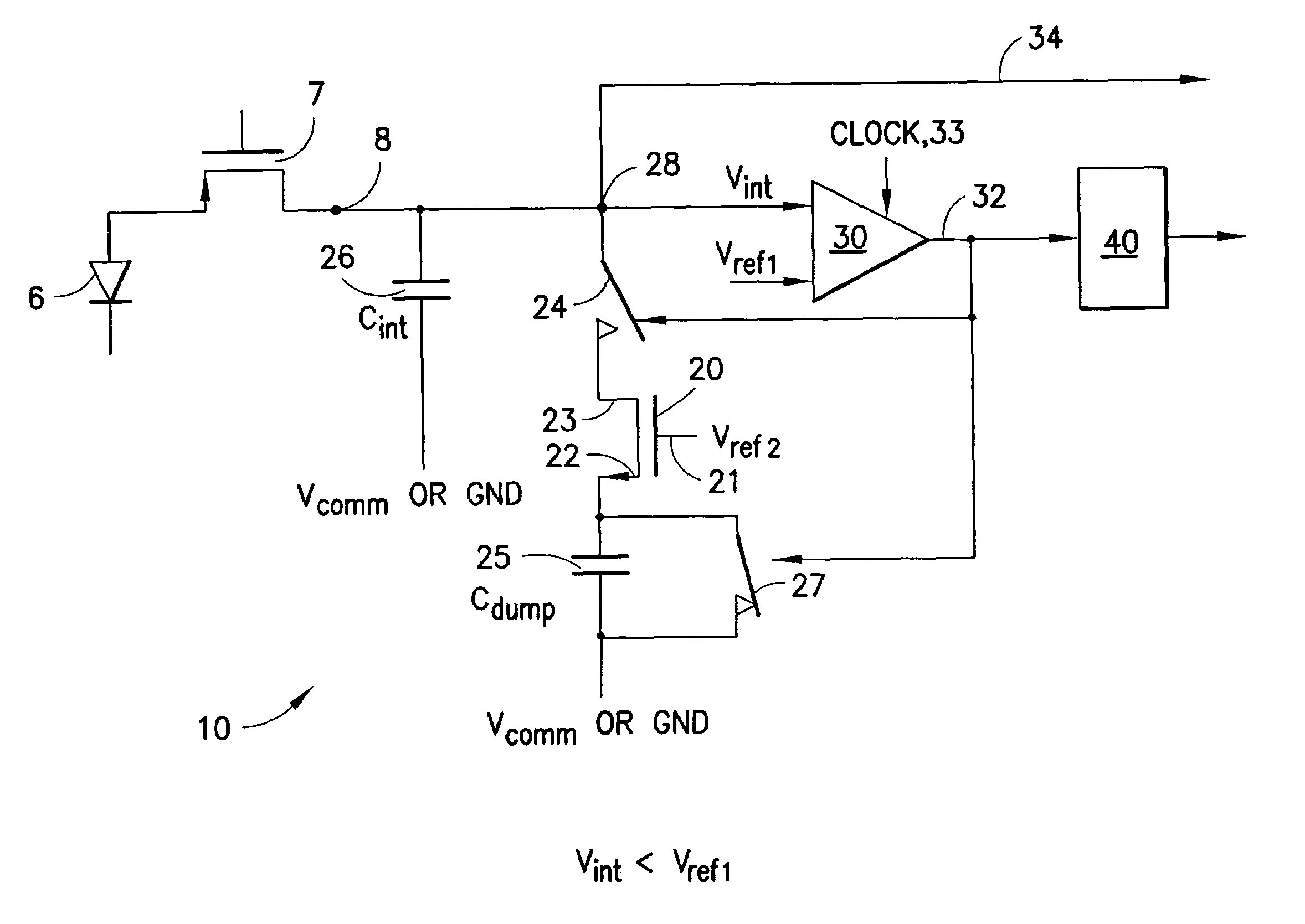
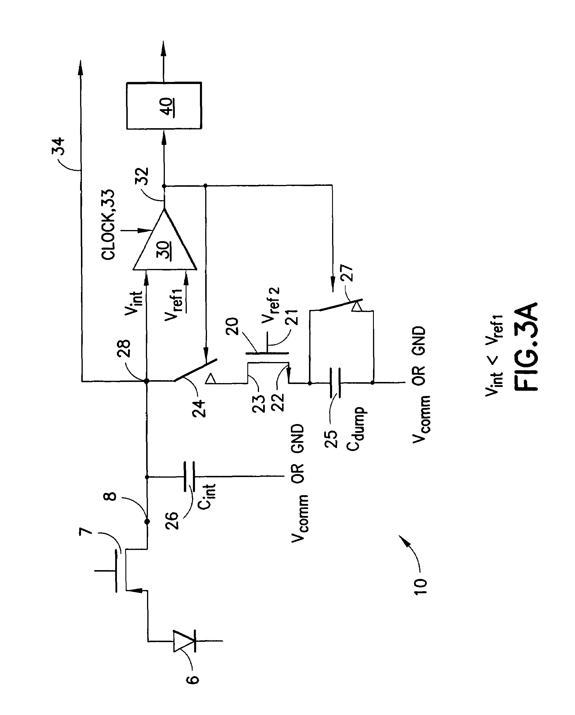
[0023]Disclosed herein is a low power delta-sigma ADC, such as one that may be used in a large imaging array. An exemplary embodiment is depicted in FIGS. 3A–B. A low power delta-sigma ADC 10 is connected by a protection FET 7 or other protection circuitry to imaging components, represented as a diode 6. An input node 8 is a point at which current from the imaging components or other such radiation detectors enters the circuit 10 substantially unchanged by the circuit 10. Imaging components 6 such as cells of an array to be described below provide an electrical signal through the protection FET 7 to the input node 8.

[0024]An integration node 28 is coupled in series with the input node 8. An integrating capacitor 26, a first switch 24, and a comparator 30 are each connected in parallel to the integration node 28. The first switch 24 is disposed between the integration node 28 and a transistor 20, herein termed an injection field effect transistor (FET) 20. The injection FET 20 includ...


PUM


Abstract

A low power delta-sigma analog to digital converter 10 for converting current mode signals without an amplifier includes an integration capacitor 26, a comparator 30, and a first switch 24 in parallel with one another and coupled to an integration node 28. A FET 20 and the first switch are disposed in series between a dump capacitor 25 and the integration node. A second switch 27 operates to discharge the dump capacitor, and an output of the comparator controls both switches in opposition. Preferably, no op-amps are included in the circuit, and current is supplied by an imaging component 5. In a first comparator state, the first capacitor charges, the first switch is open and the second switch is closed, and the dump capacitor discharges. In a comparator second state, the first switch is closed and the second switch is open, and the integration capacitor transfers a fixed amount of charge into the dump capacitor through an injection FET operating in saturation.

Description

STATEMENT REGARDING FEDERALLY SPONSORED RESEARCH OR DEVELOPMENT[0001]This invention was made with Government support under contract No. N66001-02-C-8078 awarded by the Department of the Navy. The Government has certain rights in this invention.TECHNICAL FIELD OF THE INVENTION[0002]The teachings herein relate to a low power delta-sigma analog to digital converter (ADC) that is particularly advantageous for use with sensors of an array.BACKGROUND OF THE INVENTION[0003]Delta-Sigma analog to digital converters (ADCs) work by integrating (the Sigma) the difference (the Delta) between an input signal and an output value. The integrator is embedded in a feedback loop in such a way that the difference is driven to zero, making the output (a digital bit stream or word) equal in value to the input, which is a voltage or current. Hypothetically, for an ideal integrator, the delta would be precisely zero after settling. Typically, the integration is performed by an operational amplifier and a c...

Claims


Application Information

Patent Timeline
IPC IPC(8): H03M3/00H03M3/02
CPCH03M3/32H03M3/39H03M3/43H03M3/496H03M3/456
Inventor FLETCHER, CHRISTOPHER L.SKELE, MARTINS
Owner RAYTHEON CO
Learn More