Method for forming heightened solder bumps on circuit boards

a technology of heightened solder bumps and circuit boards, which is applied in the direction of printed circuit aspects, printed circuit manufacturing, conductive pattern formation, etc., can solve the problems of difficult to achieve fine pitch demands of hollowed masks, difficult to bind with solder immediately, and thicker masks. achieve the height demands of solder bumps, improve the quality of solder bumps

Inactive Publication Date: 2005-12-27
COMPEQ MFG
View PDF1 Cites 24 Cited by
  • Summary
  • Abstract
  • Description
  • Claims
  • Application Information

AI Technical Summary

Benefits of technology

[0005]The present invention mainly provides a method for forming heightened solder bumps on a circuit board to improve qualities of the solder bumps and to achieve the height demands for the solder bumps.

Problems solved by technology

In general, the pads made of copper, gold, or silver etc. are not easily to bind with solder immediately.
In addition, the hollowed patterns of mask are hard to achieve fine pitch demands if have solder height requirement, such as bump pitch <150 um, because limitations in thickness of the mask and means to form the hollowed patterns.
In other words, the thickness of the mask is thicker, the yield of the solder bumps are poorer, namely fail in controlling the quantity of the solder paste.
Therefore, due to the limitations, the solder bumps having a height of 20 um or 20 um above are in great demand, due to some devices need more solder while soldering.

Method used


Image

  • Method for forming heightened solder bumps on circuit boards
  • Method for forming heightened solder bumps on circuit boards
  • Method for forming heightened solder bumps on circuit boards

Examples


Embodiment Construction

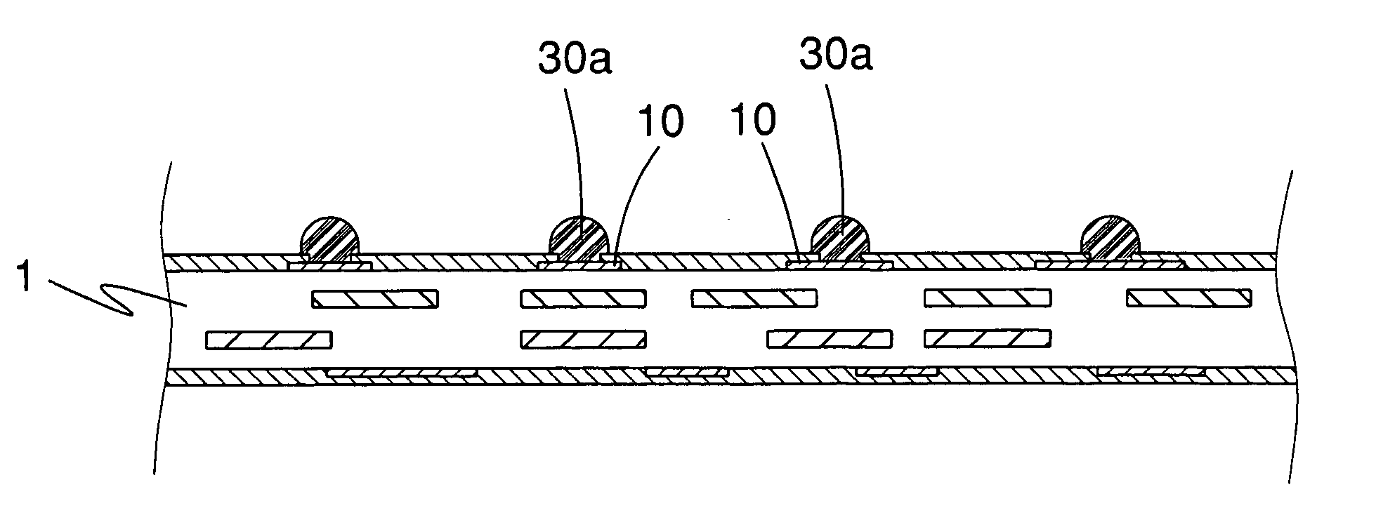
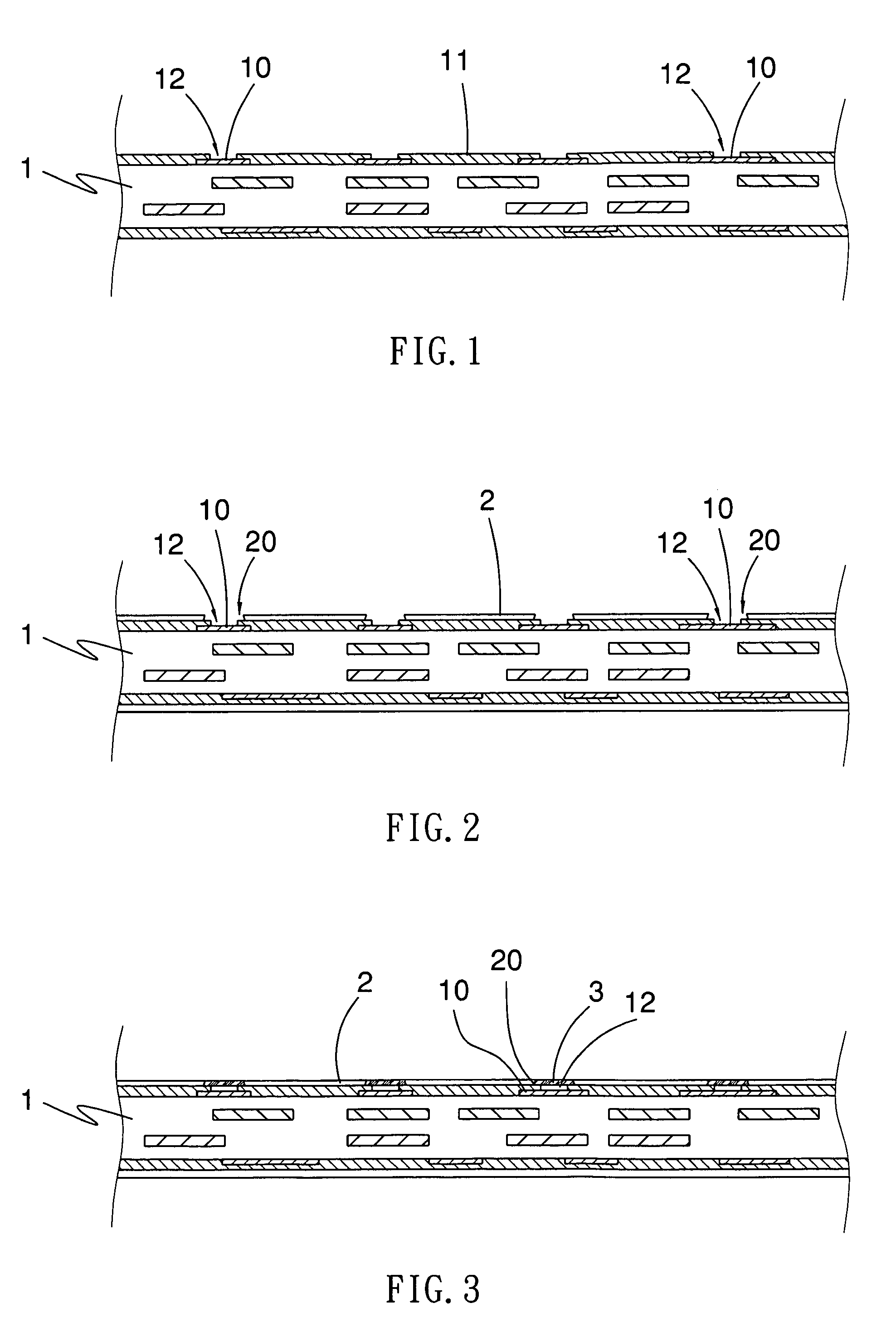
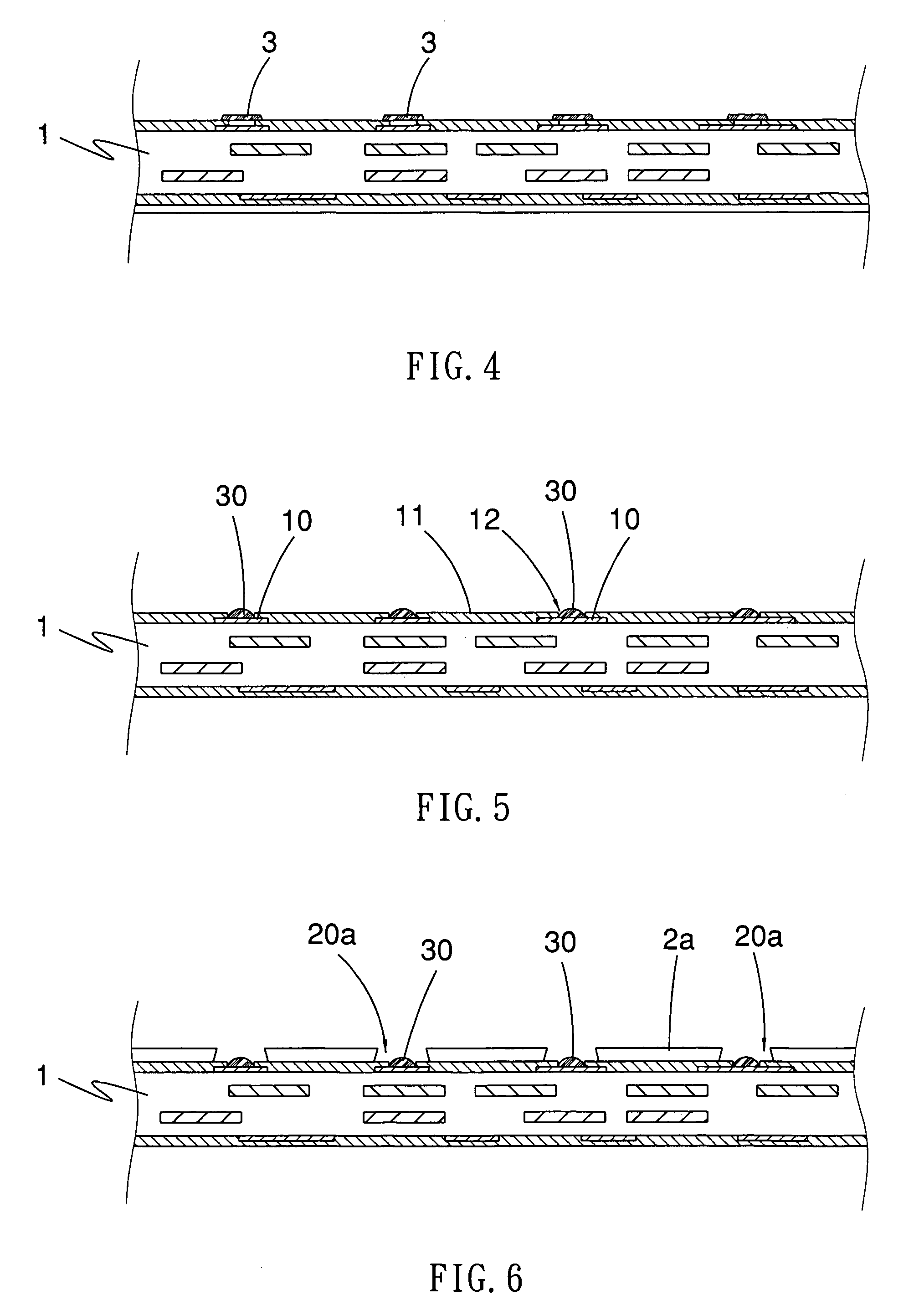
[0018]FIGS. 1–9 show a preferred embodiment of the present invention and sequential steps of a method for forming heightened solder bumps on a circuit board. In FIG. 1, the circuit board 1 is a multilayer circuit board with conductor patterns, which include a plurality of pads 10. In addition, the circuit board 1 has a surface formed with a solder resist 11 having a plurality of openings 12 for exposing the pads 10 respectively and correspondingly, so the pads could be applied to solder with electronic components.

[0019]As shown in FIG. 2, a first mask 2 is overlaid on the surface of the circuit board 1. The first mask 2 has a plurality of first holes 20, which are corresponding to the pads 10 of the circuit board 1 respectively. In FIG. 3, the first holes 20 of the first mask 2 are filled with first solder paste 3 by a squeegee (not shown) in a quick and light squeeze manner. In such manner, the quantity of the first solder paste 3 is provided for filling the first holes 20 of the f...


PUM


Abstract

The present invention relates a method for forming heightened solder bumps on a circuit board, which has a surface formed with a plurality of pads and a solder resist thereon and the pads are exposed from the solder resist. The steps of the method mainly are: firstly, applying a first stencil printing and a first reflow process to the circuit board so that a plurality of first solder bumps form on the pads respectively. Then, apply a second stencil printing and a second reflow process to the circuit board so as to have solder paste formed on the first solder bumps and to have the solder paste integrated with the first solder bumps respectively to form the heightened solder bumps on the pads.

Description

TECHNICAL FIELD[0001]The present invention generally relates to a field of circuit board manufacture and more particularly, relates to a method for forming heightened solder bumps on a circuit board.BACKGROUND OF THE INVENTION[0002]Pads exposed from solder resists are provided for soldering with surface mount devices, such as ball grid array (BGA), quad flat package (QFP) and so on. In general, the pads made of copper, gold, or silver etc. are not easily to bind with solder immediately. Therefore, the pads are usually precoated with the solder for improving solder wettability and self-alignment effect, while bumps of the BGA or a flip chip are soldered with the pads. In addition, the precoated solder generally forms with certain heights and shapes on the pads, such spherical shapes for soldering with the bumps of the BGA or the flip chip easily. Thus, the solder precoating procedure is considered as an essential procedure for the surface mounting technology.[0003]A conventional meth...

Claims


Application Information

Patent Timeline
Patent Type & Authority Patents(United States)
IPC IPC(8): H01L21/44H01L21/48H01L23/498H05K3/12H05K3/34
CPCH01L21/4867H05K3/3484H01L23/49816H05K3/1216H05K2201/035H05K2203/043H05K2203/1476H01L2924/0002H01L2924/00H05K3/3485
Inventor LIN, CHENG-YUANHUANG, TE-CHANG
Owner COMPEQ MFG
Why Eureka
Try Eureka