Power device having reduced reverse bias leakage current

a power device technology, applied in the direction of semiconductor devices, basic electric elements, electrical appliances, etc., to achieve the effect of reducing the blockage of reverse bias leakage curren

Inactive Publication Date: 2005-12-27
DIODES INC
View PDF8 Cites 28 Cited by
  • Summary
  • Abstract
  • Description
  • Claims
  • Application Information

AI Technical Summary

Benefits of technology

[0010]In accordance with the invention, a cell in a power rectifier diode having vertical current flow from one surface of a semiconductor substrate to an opposing surface includes an MOS gate structure having a shorted drain/source region and gate electrode with the entire region underlying the gate electrode being lightly doped to form a P-N junction with a drain/source region when the gate is reversed biased. The lightly doped region is shallow whereby a long channel reg...

Problems solved by technology

However, a reverse bias voltage causes the long channel inversion region to reve...

Method used


Image

  • Power device having reduced reverse bias leakage current
  • Power device having reduced reverse bias leakage current
  • Power device having reduced reverse bias leakage current

Examples


Embodiment Construction

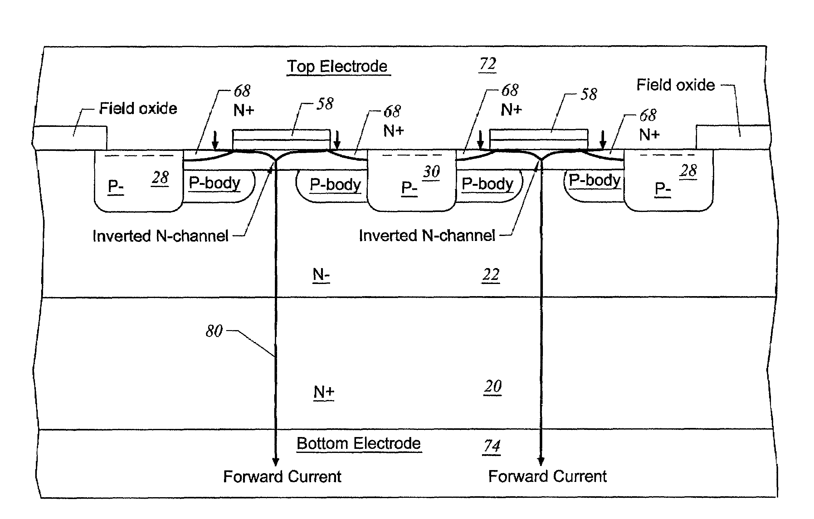
[0016]FIGS. 4–16B are section views illustrating steps in fabricating a power rectifier in accordance with the invention. The steps in FIGS. 4–13 are similar to the steps in fabricating the power rectifier devices described in the co-pending patent applications, supra, and FIGS. 14A–16B illustrate specific steps in fabricating embodiments of the present invention.

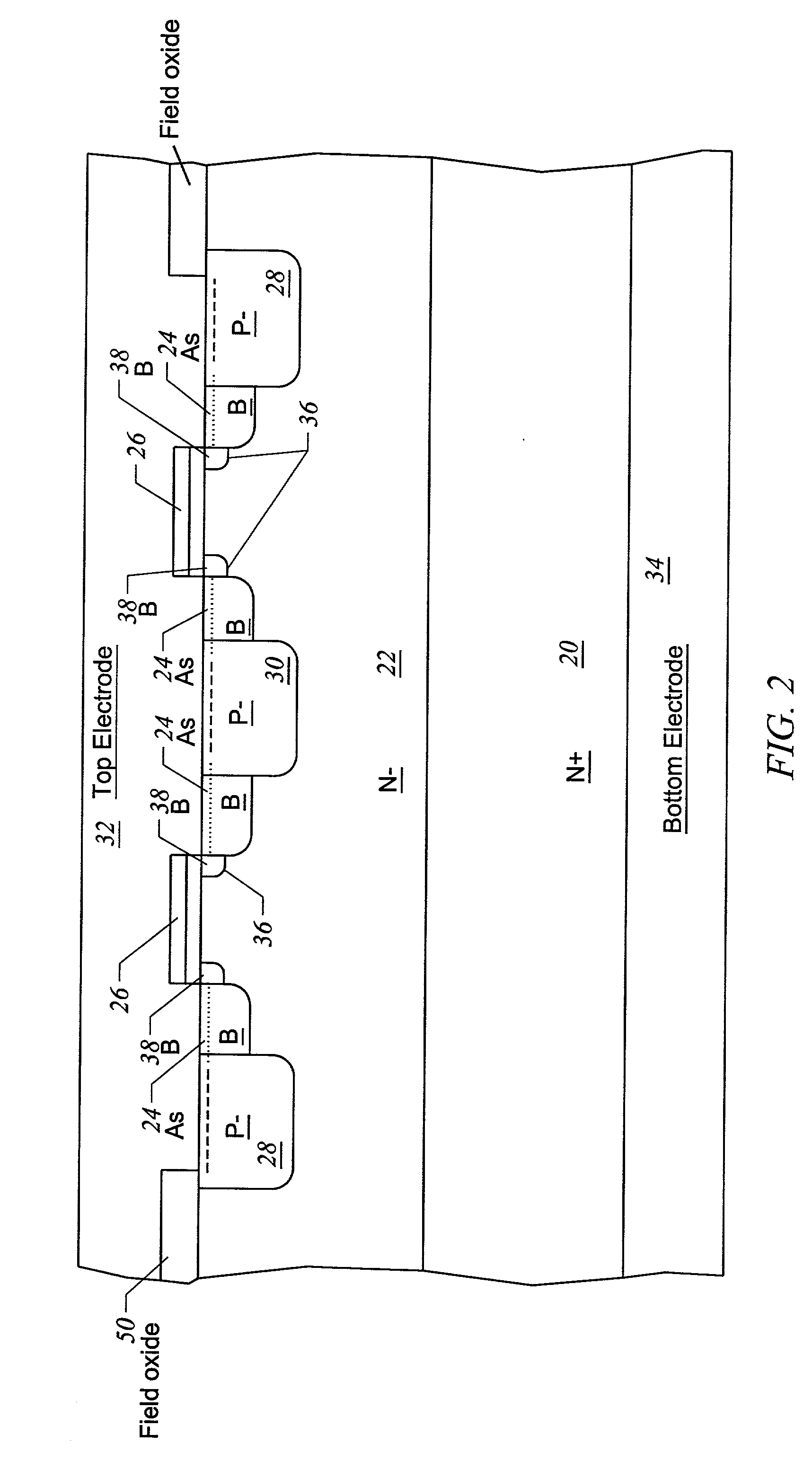
[0017]Referring to FIG. 4, a semiconductor body includes N+ substrate 20 on which is formed N− epitaxial layer 22 having a resistivity on the order of 0.1–10 ohm cm. Field oxide 50 is grown or deposited on the surface of layer 22 to a thickness of 300–1000 nm. Thereafter, as shown in FIG. 5, a photoresist pattern 52 is selectively formed over field oxide 50 by photoresist masking and etching techniques, and a P-type dopant such as boron is then implanted through openings in the photoresist. The boron can be implanted before or after photoresist removal, and as shown in FIG. 6, a boron thermal drive in forms deep P-regions i...


PUM


Abstract

A power device having vertical current flow through a semiconductor body of one conductivity type from a top electrode to a bottom electrode includes at least one gate electrode overlying a gate insulator on a first surface of the body, a channel region of second conductivity type in the surface of the body underlying all of the gate electrode, a first doped region of the second conductivity type contiguous with the channel region and positioned deeper in the body than the channel region and under a peripheral region of the gate electrode, and a second doped source/drain region in the surface of the body abutting the channel region and adjacent to the gate electrode. When the gate is forward biased, an inversion region extends through the channel region and electrically connects the first electrode and the second electrode with a small Vf near to the area between adjacent P bodies being flooded with electrons and denuded of holes. Therefore, at any forward bias this area conducts as an N-type region. When the gate electrode is reverse biased, the long channel region underlying the full length of the gate electrode reduces reverse leakage current.

Description

CROSS-REFERENCES TO RELATED APPLICATIONS[0001]This patent application is related to U.S. Pat. No. 6,186,408 issued Feb. 13, 2001, and co-pending application Ser. No. 09 / 544,730 filed Apr. 6, 2000 for Method of Fabricating Power Rectifier Device to Vary Operating Parameters in Resulting Structure; application Ser. No. 09 / 744,262 filed Dec. 19, 2000, for Multiple Fabricating Power Rectifier Device to Vary Output Parameters in Resulting Structure; application Ser. No. 09 / 805,815 filed Mar. 13, 2001 for Method of Fabricating Power Rectifier Device; and application Ser. No. 10 / 037,495 filed Jan. 2, 2002 for Power Device Having Vertical Current Path with Enhanced Pinchoff for Current Limiting, the descriptions of which are incorporated by reference for all purposes.BACKGROUND OF THE INVENTION[0002]This invention relates generally to power semiconductor devices, and more particularly the invention relates to a power semiconductor rectifier device and a method of making same.[0003]Power sem...

Claims


Application Information

Patent Timeline
IPC IPC(8): H01L21/336H01L29/10H01L29/78
CPCH01L29/1095H01L29/66712H01L29/7802H01L29/861H01L29/7811
Inventor RODOV, VLADIMIRCHANG, PAULHURTZ, GARY M.CHERN, GEENG-CHUANBAO, JIANREN
Owner DIODES INC
Why Eureka
Try Eureka