Semiconductor device having multiple substrates

a technology of semiconductor devices and substrates, applied in the direction of semiconductor/solid-state device details, acceleration measurement using interia forces, instruments, etc., can solve the problems of increased manufacturing cost, increased manufacturing cost of the device b>101/b>, and increased manufacturing cost, so as to protect from outside disturbance

Active Publication Date: 2005-12-27
DENSO CORP
View PDF5 Cites 54 Cited by
  • Summary
  • Abstract
  • Description
  • Claims
  • Application Information

AI Technical Summary

Benefits of technology

[0010]In view of the above-mentioned problems, it is an object of the present invention to provide a semiconductor device having multiple substrates. Specifically, the device is protected from outside disturbance without adding an additional shield.

Problems solved by technology

Therefore, manufacturing cost is increased.
Therefore, additional manufacturing process is necessitated so that the manufacturing cost is much increased.
Therefore, additional manufacturing process is necessitated so that the manufacturing cost of the device 101 is increased.

Method used


Image

  • Semiconductor device having multiple substrates
  • Semiconductor device having multiple substrates
  • Semiconductor device having multiple substrates

Examples


first embodiment

(First Embodiment)

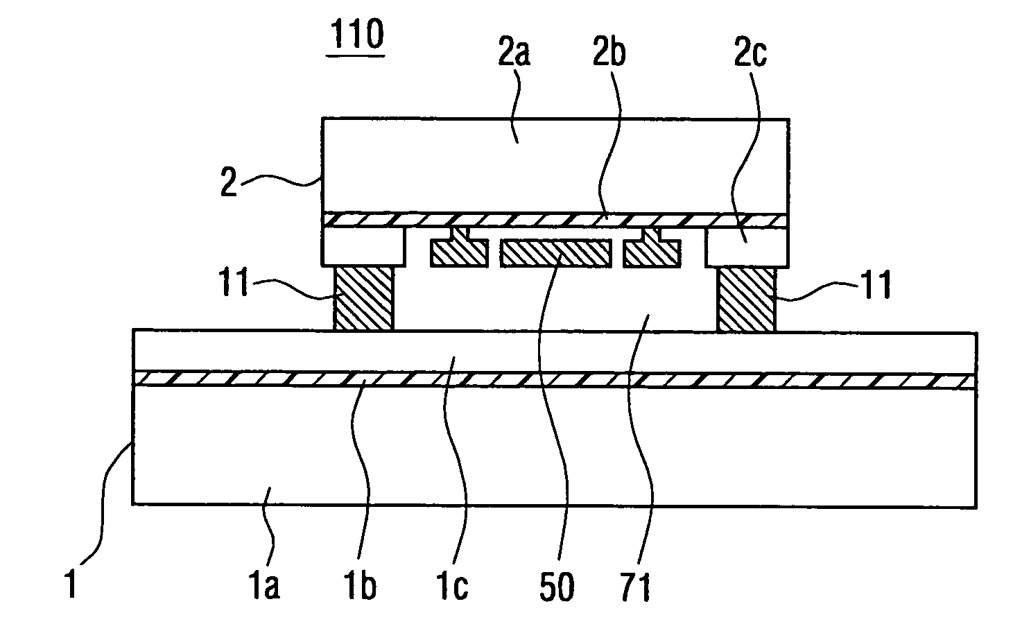
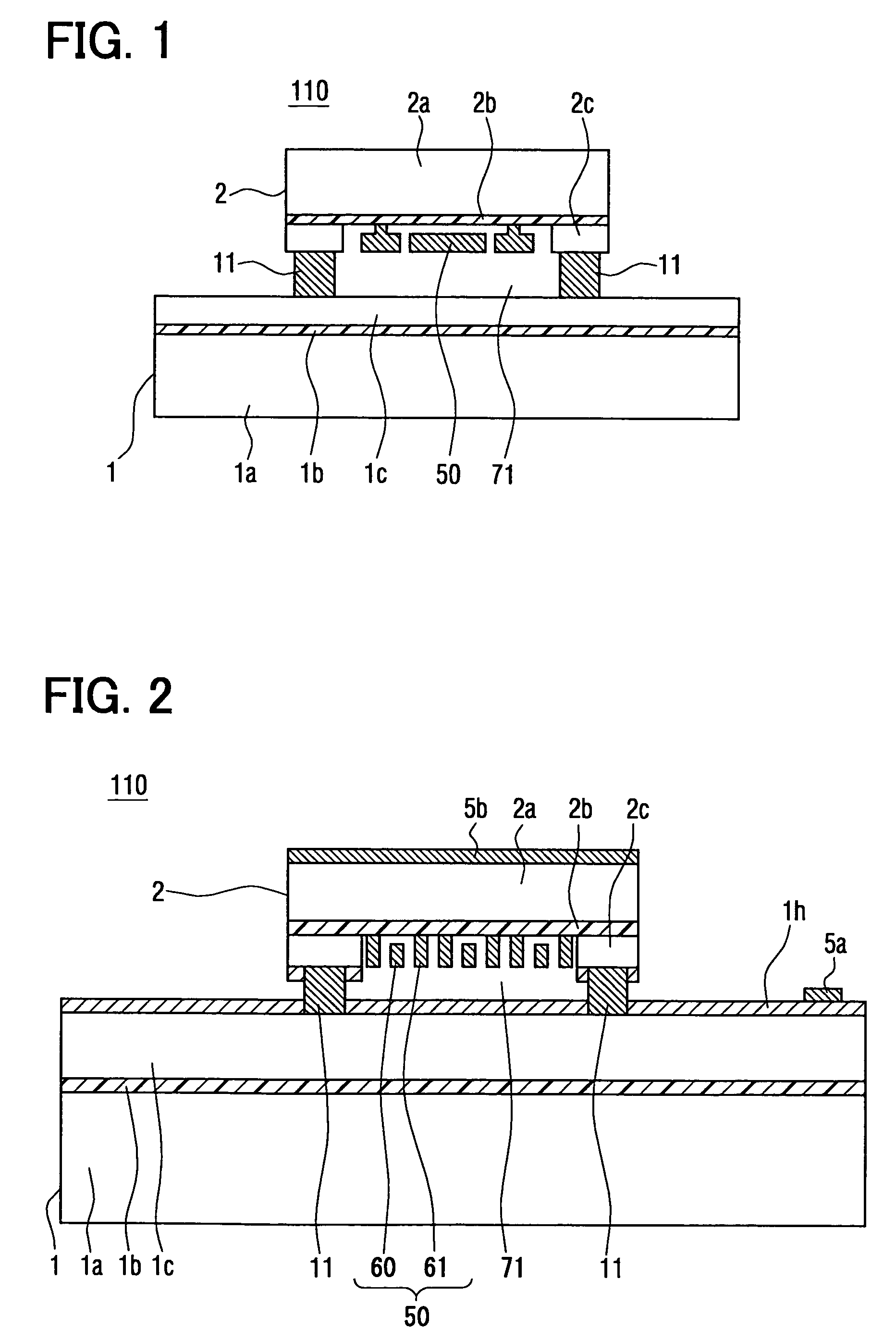
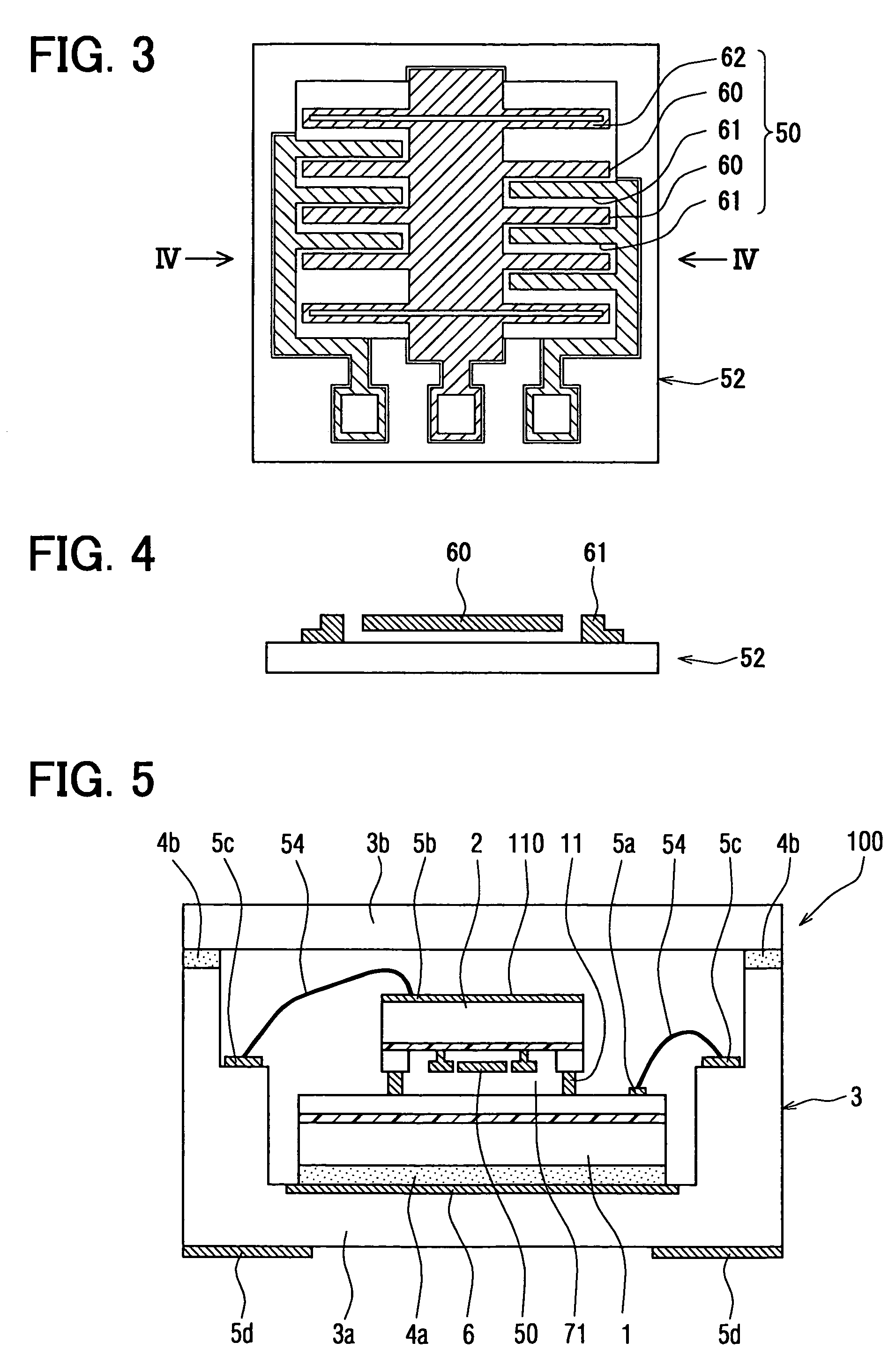
[0036]A semiconductor device 100 having a physical quantity sensor module 110 according to a first embodiment of the present invention is shown in FIGS. 1–5. The sensor module 110 includes a capacitance type semiconductor acceleration sensor. FIG. 1 shows a sensor module 110, and FIG. 2 shows the detail of the sensor module 110. The sensor module 110 includes a sensor chip 52 and a signal processor 53. The sensor chip 52 of the sensor module 110 is for example, shown in FIGS. 3 and 4. The device 100 with the sensor module 110 is shown in FIG. 5, which is a whole construction including a package for accommodating the sensor module 110 therein.

[0037]As shown in FIG. 1, the sensor module 110 includes the first and second substrate 1, 2. The first substrate 1 for providing the signal processor 53 includes the first silicon layer 1a as the first semiconductor layer, an oxide film 1b as an insulation layer, and the second silicon layer 1c as the second semiconductor laye...

second embodiment

(Second Embodiment)

[0049]A semiconductor device 200 having a sensor module 210 according to a second embodiment of the present invention is shown in FIGS. 6–7. The sensor module 210 includes the first and second loop layers 1d, 2d. The first loop layer 1d is formed in the second silicon layer 1c of the first substrate 1, which includes the signal processor 53. The second loop layer 2d is formed in the second silicon layer 2c of the second substrate 2, which includes the movable portion 50. The first loop layer 1d is electrically connected to the second loop layer 2d through a loop bump 11a.

[0050]The first loop layer 1d of the first substrate 1 is electrically insulated from the other portion of the second silicon layer 1c of the first substrate 1 by a loop insulation portion 1e, the other portion being except for the first loop layer 1d. The first poly crystalline silicon layer if is disposed between the first silicon layer 1a and the oxide film 1b. The first poly crystalline silic...

third embodiment

(Third Embodiment)

[0068]A semiconductor device 300 having a sensor module 310 according to a third embodiment of the present invention is shown in FIGS. 9 and 10. The sensor module 310 includes the first and second loop layers 1d, 2d. The first loop layer 1d is formed in the second silicon layer 1c of the first substrate 1, and the second loop layer 2d is formed in the second silicon layer 2c of the second substrate 2. The first loop layer 1d of the first substrate 1 is electrically isolated from the first silicon layer 1a of the first substrate 1 by the oxide film 1b. The second loop layer 2d of the second substrate 2 is electrically isolated from the first silicon layer 2a of the second substrate 2 by the oxide film 2b. In this embodiment, the sensor module 310 does not include the first and second poly crystalline silicon layers 1f, 2f and the first and second contact portions 1g, 2g.

[0069]As shown in FIG. 10, the movable portion 50 is formed in the second silicon layer 2c of th...


PUM


Abstract

A semiconductor device includes a first substrate including first, second and third layers; and a second substrate including fourth, fifth and sixth layers. The first substrate provides an electric device. The second substrate provides a physical quantity sensor. The first layer of the first substrate and the fourth layer of the second substrate are shields for protecting the electric device and the physical quantity sensor. The device is protected from outside disturbance without adding an additional shield.

Description

CROSS REFERENCE TO RELATED APPLICATIONS[0001]This application is based on Japanese Patent Applications No. 2003-88934 filed on Mar. 27, 2003, and No. 2003-430049 filed on Dec. 25, 2003, the disclosures of which are incorporated herein by reference.FIELD OF THE INVENTION[0002]The present invention relates to a semiconductor device having multiple substrates.BACKGROUND OF THE INVENTION[0003]A semiconductor device 101 is disclosed, for example, in Japanese Patent Application Publication No. 2001-227902 (i.e., U.S. Pat. No. 6,316,840). The device 101 includes a sensor module 111 for detecting physical quantity such as acceleration, pressure and angular rate, as shown in FIG. 17. The sensor module 111 provides an acceleration sensor, a pressure sensor or an angular rate sensor. In the sensor module 111, a movable portion 50 is disposed on a principal plane of a sensor substrate, i.e., a sensor chip 52. The sensor chip 52 includes at least the movable portion 50 and an electric device (no...

Claims


Application Information

Patent Timeline
Patent Type & Authority Patents(United States)
IPC IPC(8): G01P15/125B81B3/00B81B7/00G01P1/02G01P15/08H01L23/00H01L23/12H01L23/50H01L23/552H01L25/065H01L29/76H01L29/84H01L31/062
CPCB81B7/0058G01P1/023G01P15/0802G01P15/125H01L2224/48091H01L2224/48247H01L2924/00014H01L2924/10253H01L2924/00H01L2924/3025H01L2924/181B81B2207/012H01L2924/00012
Inventor FUJII, TETSUO
Owner DENSO CORP
Why Eureka
Try Eureka