
Bipolar transistor having self-aligned silicide and a self-aligned emitter contact border
a bipolar transistor and contact border technology, applied in the field of bipolar transistors, can solve the problem of high base resistance (rb) and achieve the effect of reducing the emitter resistan
- Summary
- Abstract
- Description
- Claims
- Application Information
AI Technical Summary
Benefits of technology
Problems solved by technology
Method used
Image

Examples
Embodiment Construction
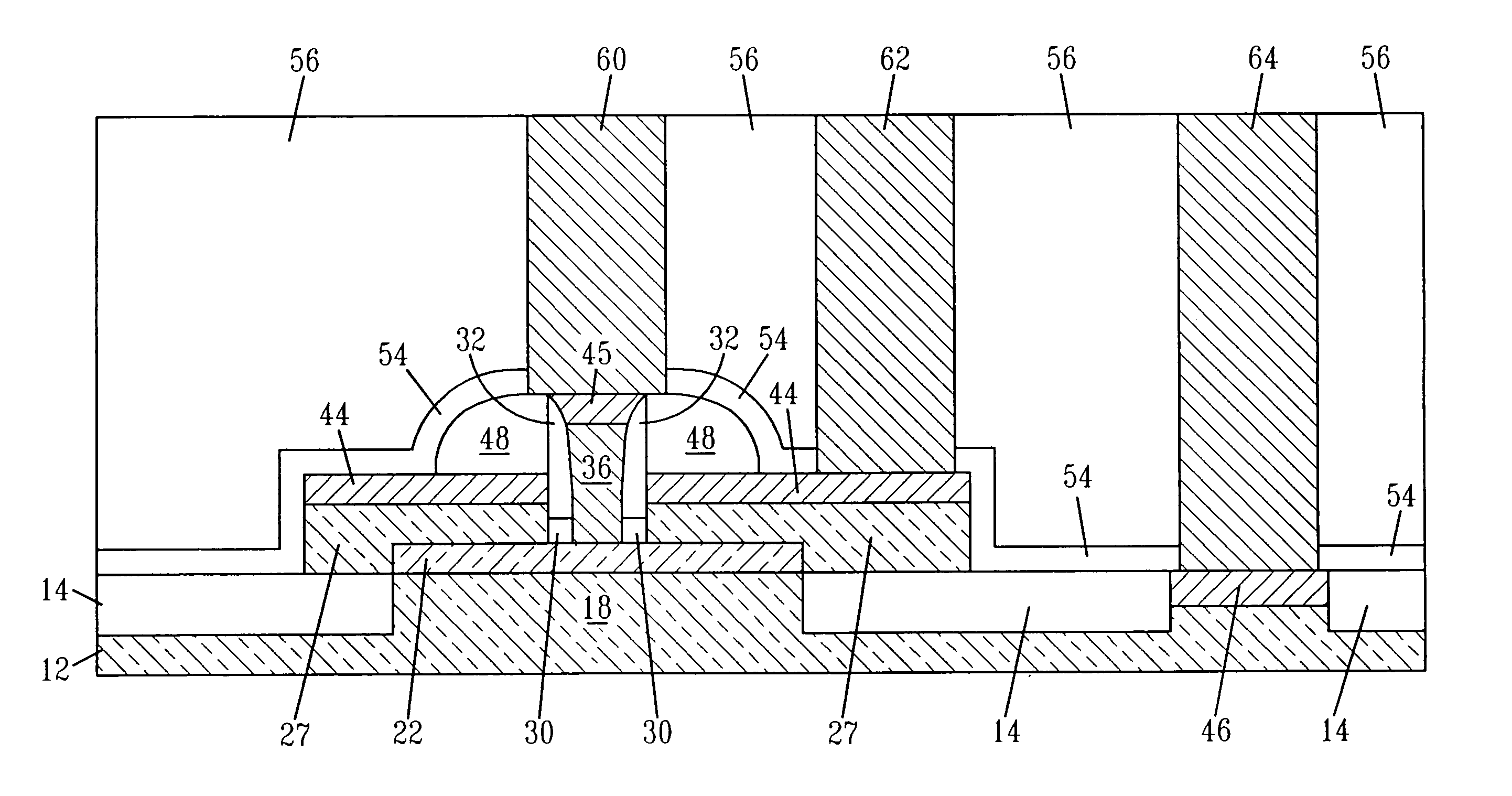
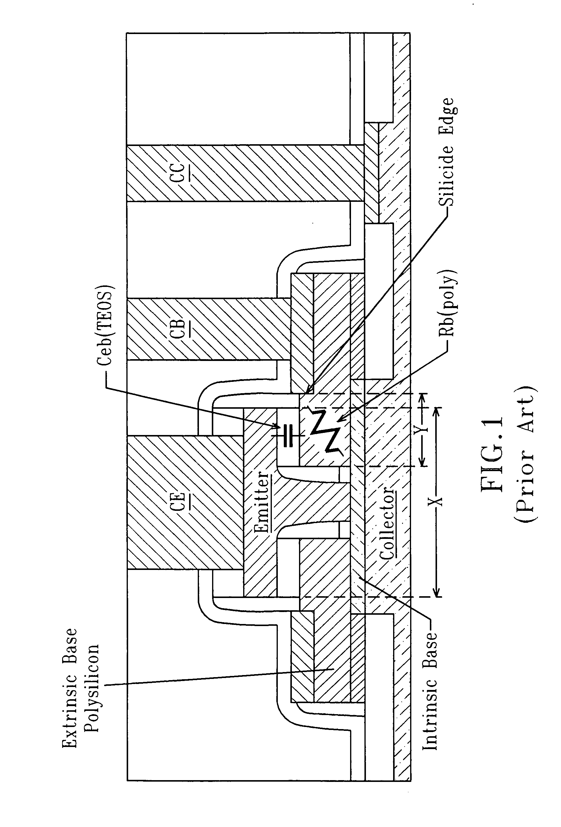
[0052]The present invention, which provides bipolar transistors having self-aligned silicides and self-aligned emitter contact border as well as methods of fabricating the same, will now be described in greater detail by referring to the drawings that accompany the present application. In the accompanying drawings, like and / or corresponding elements are referred to by like reference numerals.
[0053]The drawings of the present application illustrate only the heterojunction bipolar transistor (HBT) area. For clarity, the CMOS device areas as well as other areas of a typical BiCMOS structure are not shown in drawings. These other areas not shown lay to the periphery of the HBT area shown. Additionally, although a single HBT device area is shown, the present invention can be used in forming a plurality of HBTs on top of a single substrate.
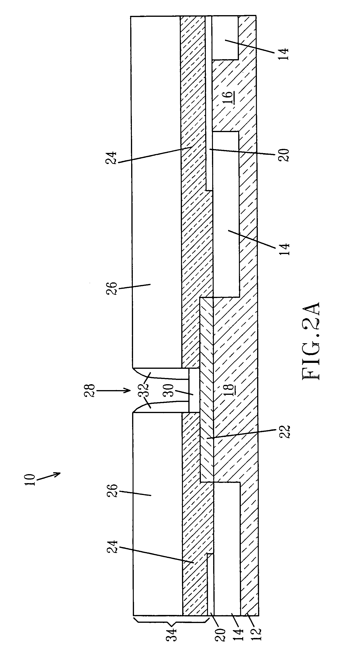
[0054]Reference is first made to FIGS. 2A–2H which illustrate a first embodiment of the present invention. In this embodiment, a block polysilicon emit...
PUM
 Abstract
Description
Claims
Application Information