Display apparatus, image control semiconductor device, and method for driving display apparatus

Active Publication Date: 2005-12-27
JAPAN DISPLAY CENT INC
View PDF11 Cites 37 Cited by
  • Summary
  • Abstract
  • Description
  • Claims
  • Application Information

AI Technical Summary

Benefits of technology

[0014]The present invention is made in consideration of the above-mentioned problems. It is an object of the invention to provide a display apparatus in which a reduction in size can be realized, w

Problems solved by technology

In the conventional display apparatus, since the driving circuit is constructed by using a plurality of circuits such as graphic controller IC 101, gate array 102, signal line driving circuit, and scanning line driving circuit, there is such a problem that the scale of the driving circuit cannot be reduced.
When the resolution is raised

Method used


Image

  • Display apparatus, image control semiconductor device, and method for driving display apparatus
  • Display apparatus, image control semiconductor device, and method for driving display apparatus
  • Display apparatus, image control semiconductor device, and method for driving display apparatus

Examples


Example

Second Embodiment

[0153]According to a second embodiment, there is provided an apparatus intended for a reduction in power consumption by arranging data buses from substantially the center in the lateral direction of an EL panel portion toward both the ends thereof.

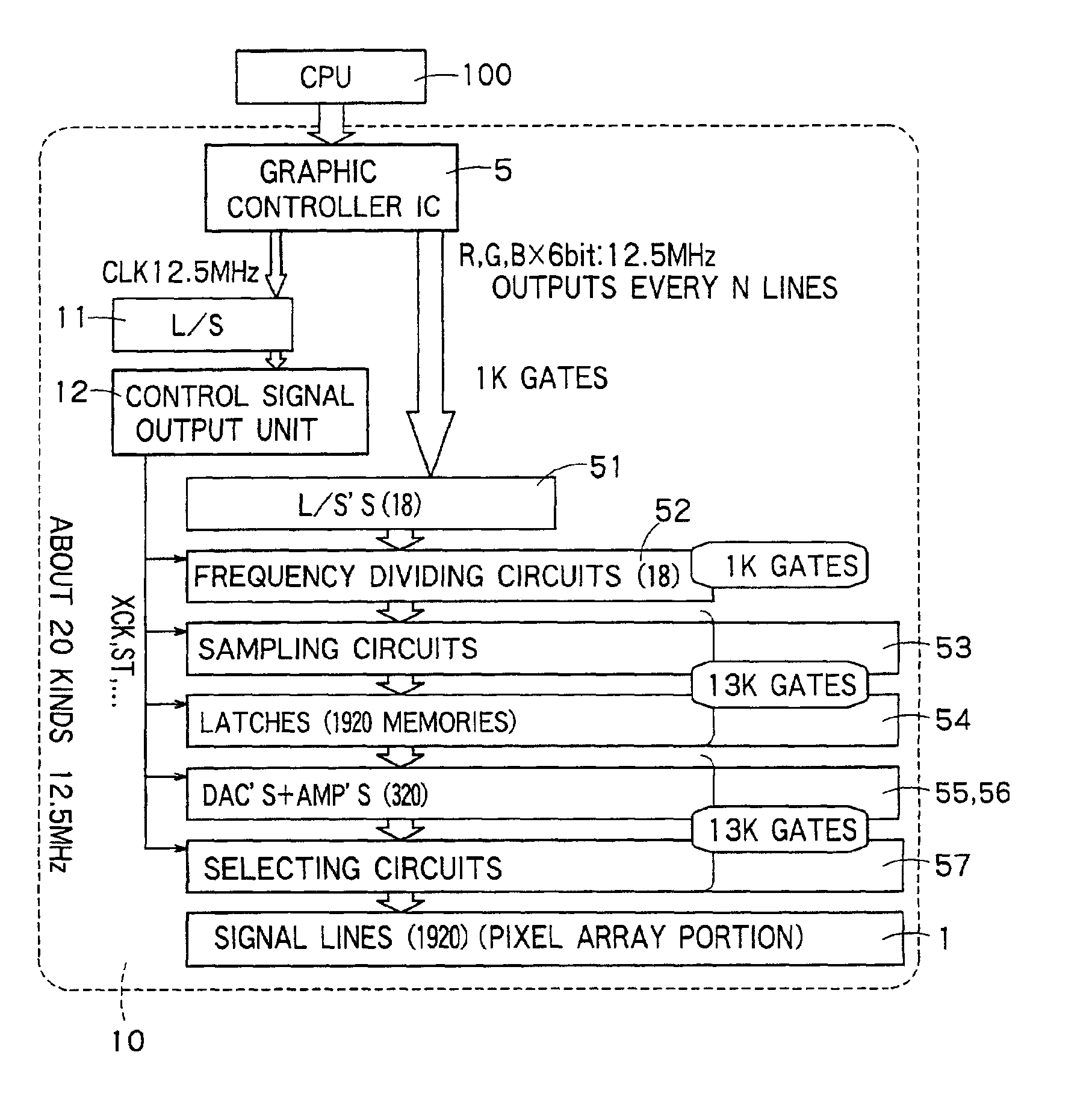
[0154]FIG. 16 is a block diagram of a display apparatus of the second embodiment according to the present invention. The display apparatus in FIG. 16 has an EL panel portion 201 formed on a glass substrate and a controller IC 202 mounted on the glass substrate or another substrate.

[0155]The EL panel portion 201 comprises: a pixel array portion 203 in which the display gray scale luminance of the pixel can be controlled on the basis of a memory comprising a plurality of bits provided for each pixel; an I / F circuit 204 for transmitting and receiving signals to / from the controller IC 202; data buses 205a and 205b arranged from substantially the center in the lateral direction of the pixel array portion 203 toward both the end...

Example

Third Embodiment

[0187]According to a third embodiment, signal lines are divided into four blocks and data buses are provided for each block.

[0188]FIG. 27 is a block diagram showing the schematic construction of a signal line driving circuit when signal lines are divided into four blocks B1 to B4 and are driven. As shown in the diagram, 160 signal lines for each of RGB are provided for each block and exclusive-use data buses DB1 to DB4 are provided for respective blocks.

[0189]First, red odd pixel data of one horizontal line is supplied to the data buses DB1 to DB4 and, after that, red even pixel data is supplied to them. Subsequently, green odd pixel data is supplied and then green even pixel data is supplied. After that, blue odd pixel data is supplied and then blue even pixel data is supplied.

[0190]The level of the digital pixel data on the data buses DB1 to DB4 are converted by the level shifters 51. After that, they are latched by the sampling latches 53. (80 pixels×6 bits=) 480 ...


PUM


Abstract

It is an object of the present invention to provide a display apparatus which can be miniaturized and is operated stably even at high resolution.
The display apparatus according to the present invention includes a pixel array unit, a signal line driving circuit, and a scanning line driving circuit, each of which is formed by using a polysilicon TFT on a glass substrate, a control circuit, and a graphic controller IC. Since the graphic controller IC rearranges digital pixel data DATA in the inside, it is unnecessary to provide a gate array. Since the cycle of a clock signal CLK is twice as much as that of the digital pixel data DATA, the clock signal CLK having a frequency at which the polysilicon TFT normally operates can be supplied to the signal line driving circuit. Further, since the edge of the clock signal CLK is deviated from the changing position of the digital pixel data DATA and they are outputted, the signal line driving circuit can effectively capture the digital pixel data DATA.

Description

CROSS REFERENCE TO RELATED APPLICATIONS[0001]This application claims benefit of priority under 35USC § 119 to Japanese Patent Application No. 2000-127093 filed on Apr. 27, 2000, No. 2000-321530 filed on Oct. 20, 2000, and No. 2001-123191 filed on Apr. 20, 2001, the entire contents of which are incorporated by reference herein.BACKGROUND OF THE INVENTION[0002]1. Field of the Invention[0003]The present invention relates to a display apparatus in which display elements and a driving circuit are formed on the same insulating substrate, an image control semiconductor device, and a method for driving the display apparatus.[0004]2. Related Background Art[0005]A display apparatus in which a large number of display elements were arranged laterally and longitudinally on an insulating substrate has been known. As a representative example, there is a liquid crystal display apparatus.[0006]In this kind of conventional display apparatus, separately from a pixel array substrate on which the displa...

Claims


Application Information

Patent Timeline
IPC IPC(8): G02F1/133G09F9/00G09G3/20G09G3/32G09G3/36G09G5/00G09G5/36
CPCG09G3/3648G09G3/3688G09G5/363G09G3/3208G09G5/006G09G2300/0408G09G2300/0857G09G2310/027G09G2310/0297G09G3/36
Inventor NAKAMURA, TAKASHIHARADA, NOZOMU
Owner JAPAN DISPLAY CENT INC
Why Eureka
Try Eureka