Wafer level package and multi-package stack

a wafer level and stack technology, applied in the field multi-package stacks of wafer level packages, can solve the problems of fissures and other defects, relatively high manufacturing cost of packages, and unreliable solder ball joints

Active Publication Date: 2006-01-03
SAMSUNG ELECTRONICS CO LTD
View PDF29 Cites 148 Cited by
  • Summary
  • Abstract
  • Description
  • Claims
  • Application Information

AI Technical Summary

Problems solved by technology

One disadvantage of CSP technology, however, is that the packages are relatively expensive to manufacture, especially when compared to more conventional and commonly used plastic packages, such as a ball grid array (BGA) package and a thin small outline package (TSOP).
Unfortunately, however, the solder ball joints tend to be unreliable.
The different rates of expansion of the WLP and PCB connected at opposite sides of the solder balls create mechanical stresses within the solder balls, sometimes resulting in fissures and other defects.
As a result, the joints formed by the solder balls 3a are unreliable and prone to failures.

Method used


Image

  • Wafer level package and multi-package stack
  • Wafer level package and multi-package stack
  • Wafer level package and multi-package stack

Examples


Embodiment Construction

[0029]The present invention will be described in detail below by way of several non-limiting preferred embodiments.

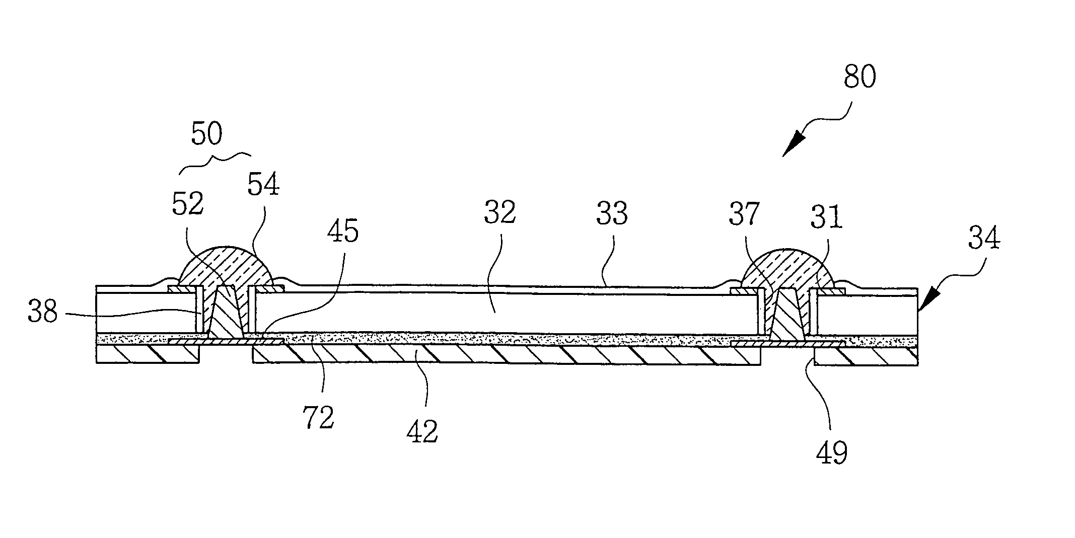
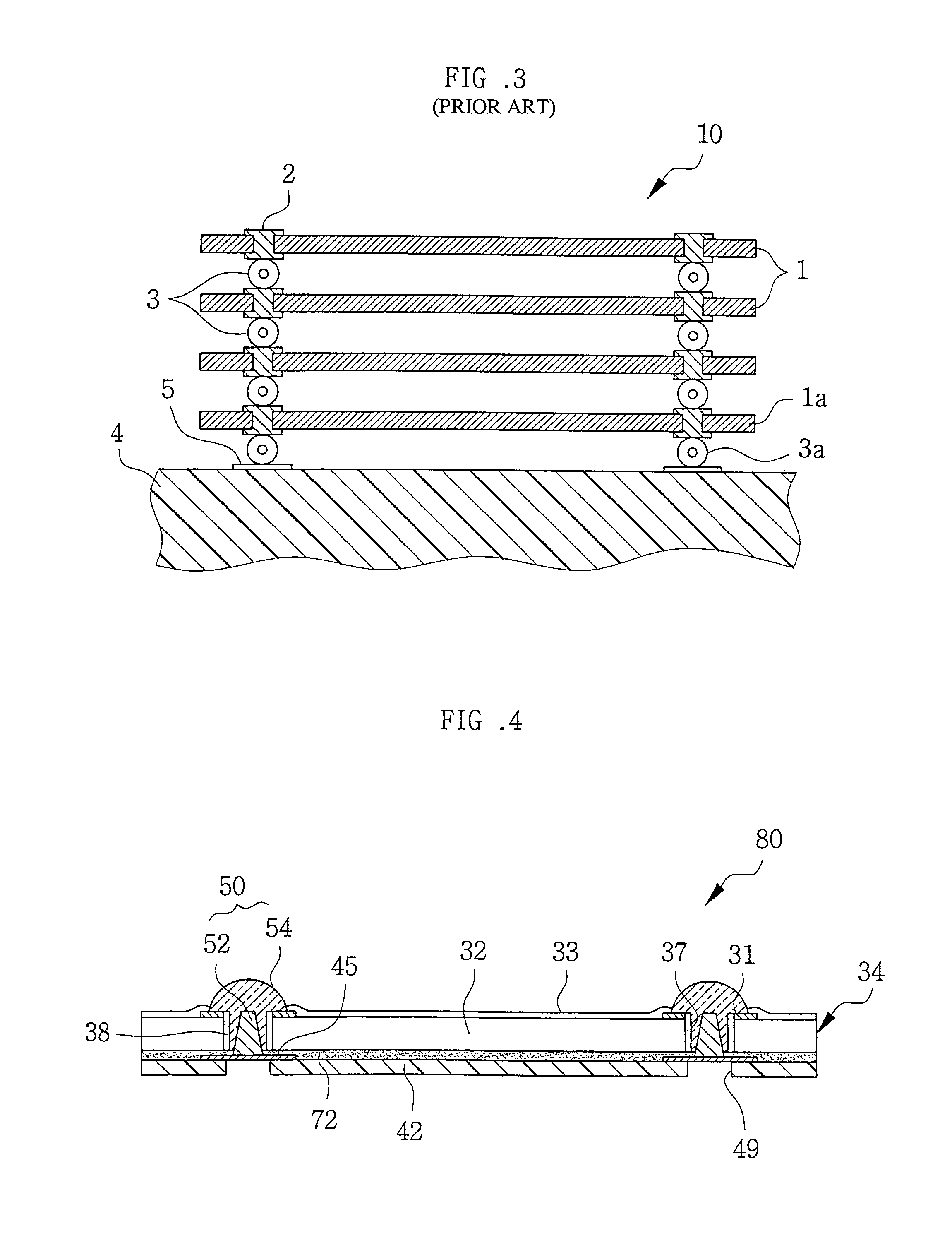
[0030]FIG. 4 is a cross-sectional view of a wafer level package (WLP) 80 in accordance with an embodiment of the present invention. The WLP 80 includes a semiconductor chip 34 which is generally defined by a semiconductor substrate 32 having a passivation layer 33 on an active upper surface of the substrate 32. Examples of the passivation layer 33 include silicon oxide, silicon nitride, and composites thereof.

[0031]At least one through hole 37 is defined through the chip 34 from the active upper surface to an inactive lower surface of the chip 34. Also, a conductive chip pad 31 at least partially surrounds each through hole 37 on the active first surface of the semiconductor chip 34. For example, the conductive chip pad 31 may be formed of aluminum.

[0032]The WLP 80 also includes a printed circuit board (PCB) 42 having an upper surface attached to the inactive lower surf...


PUM


Abstract

A semiconductor chip package includes a semiconductor chip having a through hole extending there through from an active first surface to an inactive second surface. A first conductive pad at least partially surrounds the through hole on the active first surface of the semiconductor chip. The package also includes a printed circuit board having a first surface attached to the inactive second surface of the semiconductor chip, and a second conductive pad aligned with the through hole of the semiconductor chip. A conductive material fills the through hole and contacts the first and second conductive pads.

Description

BACKGROUND OF THE INVENTION[0001]1. Field of the Invention[0002]The present invention generally relates to the packaging of semiconductor chips. More particularly, the present invention relates to wafer level packages, multi-package stacks of wafer level packages, and methods of manufacturing wafer level packages and multi-package stacks.[0003]2. Background of the Invention[0004]The miniaturization of electronic devices has led to the development of different techniques for containing semiconductor integrated circuit (IC) chips in smaller and smaller packages. The Joint Electronic Device Engineering Council (JEDEC) has proposed the name “Chip Scale Package (CSP)” to denote a semiconductor chip package which is nearly as small as the semiconductor chip itself. In particular, the JEDEC defines CSP as a package having an outline that is 1.2 times or less the outline of the semiconductor chip contained in the package. CSP technology is suitable for packaging ICs used in electronic produ...

Claims


Application Information

Patent Timeline
Patent Type & Authority Patents(United States)
IPC IPC(8): H01L23/48H01L23/12H01L23/498H01L25/065
CPCH01L23/481H01L23/49816H01L24/13H01L24/10H01L25/0657H01L2224/13099H01L2224/16H01L2225/06517H01L2225/0652H01L2225/06541H01L2225/06572H01L2225/06593H01L2924/01004H01L2924/01013H01L2924/01015H01L2924/01029H01L2924/01033H01L2924/01039H01L2924/01078H01L2924/01079H01L2924/01082H01L2924/14H01L2924/1433H01L2924/01005H01L2924/01006H01L2924/014H01L2924/00H01L2924/12042H01L2224/13H01L2224/05022H01L2224/05001H01L2224/05548H01L2224/056H01L2224/14181H01L24/03H01L2224/02377H01L24/05H01L2924/00014H01L2224/05124H01L23/12
Inventor KIM, HYEONG-SEOBCHUNG, TAE-GYEONG
Owner SAMSUNG ELECTRONICS CO LTD
Why Eureka
Try Eureka