Semiconductor storage device and portable electronic equipment having the same

a storage device and semiconductor technology, applied in the direction of digital storage, transistors, instruments, etc., can solve the problems of increasing the number of charge pump circuits, affecting the miniaturization of memory cells, and difficulty in effectively reducing the thickness of insulation films, etc., to achieve easy miniaturization, reduce manufacturing costs, and high functions

Inactive Publication Date: 2006-01-10
SHARP KK
View PDF15 Cites 32 Cited by
  • Summary
  • Abstract
  • Description
  • Claims
  • Application Information

AI Technical Summary

Benefits of technology

[0049]The portable electronic equipment having the above-mentioned construction has the semiconductor storage device that can retain the storage of two bits or more per transistor and

Problems solved by technology

Therefore, it has been difficult to effectively reduce the thickness of the insulation film 907 and the gate insulation film, and this has hindered the min

Method used


Image

  • Semiconductor storage device and portable electronic equipment having the same
  • Semiconductor storage device and portable electronic equipment having the same
  • Semiconductor storage device and portable electronic equipment having the same

Examples


first embodiment

[0125](First Embodiment)

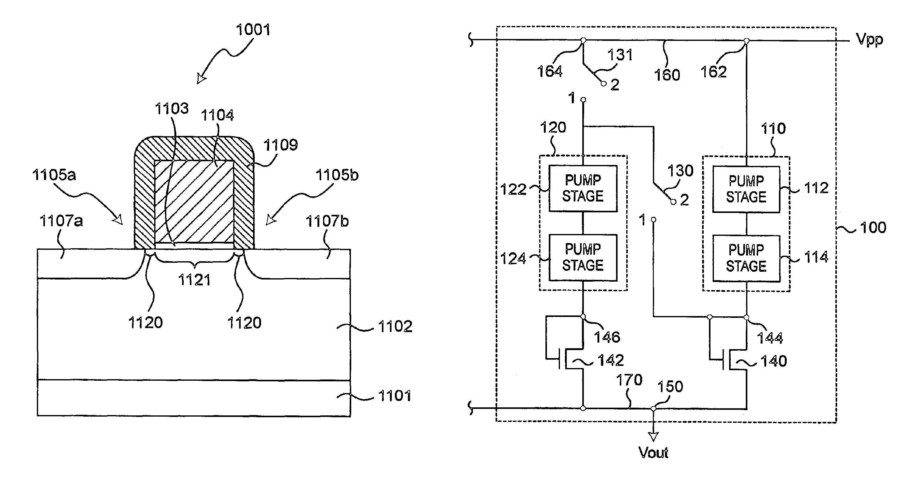
[0126]The semiconductor storage device of this embodiment is provided with a memory element 1001 that serves as one example of the nonvolatile memory element as shown in FIG. 1.

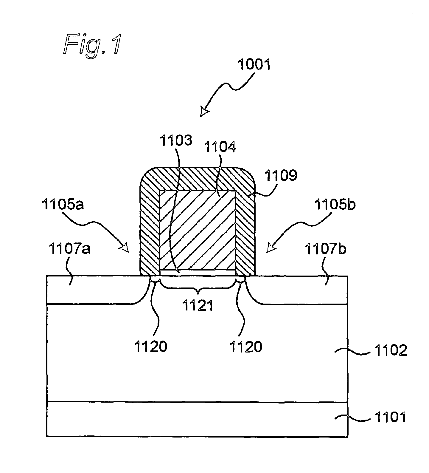
[0127]In the memory element 1001, a gate electrode 1104 is formed on a P-type well region 1102 formed via a gate insulation film 1103 on the surface of a semiconductor substrate 1101. A silicon nitride film 1109, which has a trap level for retaining electric charges and serves as a charge retaining film, is arranged on the upper surface and the side surfaces of the gate electrode 1104, and the portions of the silicon nitride film 1109 located on both side walls of the gate electrode 1104 serve as memory function bodies 1105a and 1105b for actually retaining electric charges. In this case, the memory function body means a portion where electric charges are actually accumulated by the rewrite operation in the memory function body or the charge retaining film. N-type diffusion regions 110...

second embodiment

[0150](Second Embodiment)

[0151]As shown in FIG. 8, the memory element in the semiconductor storage device of the present embodiment has a construction substantially similar to that of the memory element 1001 of FIG. 1 except for the memory function bodies 1261 and 1262 are constructed of a region for retaining electric charges (this may be a region for storing electric charges, or a film having the function to retain electric charges) and a region for restraining the escape of electric charges (this may be a film that has a function to restrain the escape of electric charges).

[0152]From the point of view of improving the retention characteristic of the memory, the memory function body should preferably include a charge retaining film having the function to retain electric charges and an insulation film. This embodiment employs a silicon nitride film 1242 that has a level for trapping electric charges as a charge retaining film and silicon oxide films 1241 and 1243 that have the oper...

third embodiment

[0167](Third Embodiment)

[0168]In this embodiment, a silicon nitride film 1242 as a film made of a first insulator in the charge holding portion 1262 has an approximately uniform film thickness as shown in FIG. 13. Further, the silicon nitride film 1242 as a charge holding film is configured such that a region 1281 having a constant thickness and disposed approximately parallel to the surface of the gate insulating film 1214 and a region 1282 extending in direction approximately parallel to the side face of the gate electrode 1217.

[0169]When a positive voltage is applied to the gate electrode 1217, electric line of force in the memory function body 1262 passes the silicon nitride film 1242 total two times through the first portion 1281 and the second portion 1282 as shown with an arrow 1283. It is noted that when a negative voltage is applied to the gate electrode 1217, the direction of electric line of force is reversed. Herein, a dielectric constant of the silicon nitride film 1242...


PUM


Abstract

A semiconductor storage device has a variable-stage charge pump, and a memory cell array to which an output from an output line of the variable-stage charge pump is fed. In the variable-stage charge pump, first and second charge pumps are connected in parallel between a common input bus and a common output bus. A first n-channel MOSFET is provided on a line connecting an output terminal of the first charge pump and the common output bus, and another n-channel MOSFET is provided on a line connecting the second charge pump and the common output bus. First switches are provided between the output terminal of the first charge pump and the first n-channel MOSFET, and between the input terminal of the second charge pump and the second switch. A second switch is provided on a line connecting an input terminal of the second charge pump and the common input bus.

Description

[0001]This nonprovisional application claims priority under 35 U.S.C. §119(a) on Patent Applications Nos. 2003-85087 and 2003-142318 filed in Japan on Mar. 26, 2003 and May 20, 2003, respectively, the entire contents of which are hereby incorporated by reference.BACKGROUND OF THE INVENTION[0002]The present invention relates to a semiconductor storage device and portable electronic equipment that employs the semiconductor storage device.[0003]Conventionally, a flash memory has typically been used as a nonvolatile semiconductor storage device.[0004]In this flash memory, as shown in FIG. 26, a floating gate 902, an insulation film 907 and a word line (control gate) 903 are formed in this order via a gate insulation film 908 on a semiconductor substrate 901, and a source line 904 and a bit line 905 are formed on both sides of the floating gate 902, constituting a memory cell. Around this memory cell are formed element isolation regions 906 (refer to JP 5-304277 A).[0005]The memory cell ...

Claims


Application Information

Patent Timeline
IPC IPC(8): G11C7/00G11C16/04G11C16/06G11C16/02G11C16/30H01L21/8247H01L27/10H01L27/115H01L29/788H01L29/792
CPCG11C16/30
Inventor TOKUI, KEIIWATA, HIROSHIYAOI, YOSHIFUMISHIBATA, AKIHIDENAWAKI, MASARU
Owner SHARP KK
Why Eureka
Try Eureka