Delay time calculation apparatus and integrated circuit design apparatus

a technology of delay time calculation and integrated circuit, which is applied in the field of delay time calculation apparatus and integrated circuit design apparatus, can solve the problem of not being able to calculate and achieve the effect of accurately calculating the delay time of the ga

Inactive Publication Date: 2006-01-10
RENESAS TECH CORP
View PDF10 Cites 4 Cited by
  • Summary
  • Abstract
  • Description
  • Claims
  • Application Information

AI Technical Summary

Benefits of technology

[0032]The present invention is implemented to solve the foregoing problem. It is therefore an object of the present invention to provide a delay time calculation apparatus and integrated circuit design apparatus capable of calculating the delay time of a gate accurately.
[0033]According to a first aspect of the present invention, there is provided a delay time calculation apparatus including: a resistance-capacitance determining section for determining, referring to the placement and routing results obtained by a placement and routing result acquiring section, a source resistance and a diffusion capacitance of a target gate of delay time calculation before a process variation, and a wiring resistance and a wiring capacitance of a wire connected to the gate after the process variation; and a delay time calculating section for calculating the delay time of the gate according to results determined by the resistance-capacitance determining section. Thus, it offers an advantage of being able to calculate the delay time of the gate accurately.
[0034]According to a second aspect of the present invention, there is provided an integrated circuit design apparatus including: a resistance-capacitance determining section for determining, referring to the placement and routing results obtained by a placement and routing result acquiring section, a source resistance and a diffusion capacitance of a target gate of delay time calculation before a process variation, and a wiring resistance and a wiring capacitance of a wire connected to the gate after the process variation; a delay time calculating section for calculating the delay time of the gate according to results determined by the resistance-capacitance determining section; and a verifying section for verifying the placement and routing results by the placement and routing section, referring to the delay time calculated by the delay time calculating section. Thus, it offers an advantage of being able to alter the placement and the like if the results of the placement and routing have something unsatisfactory.

Problems solved by technology

However, the conventional delay time calculation apparatus calculates the gate delay time after the process variation without using the actual values after the process variation.
Although it can calculate the delay time of the gate accurately when the process variation coefficients KPcell(max) and KPcell(min) for the cell delay and the process variation coefficients KPWire(max) and KPWire(min) for the wiring match the target gate of the delay time calculation, it cannot calculate the delay time of the gate when the errors of the process variation coefficients increase.

Method used


Image

  • Delay time calculation apparatus and integrated circuit design apparatus
  • Delay time calculation apparatus and integrated circuit design apparatus
  • Delay time calculation apparatus and integrated circuit design apparatus

Examples


embodiment 1

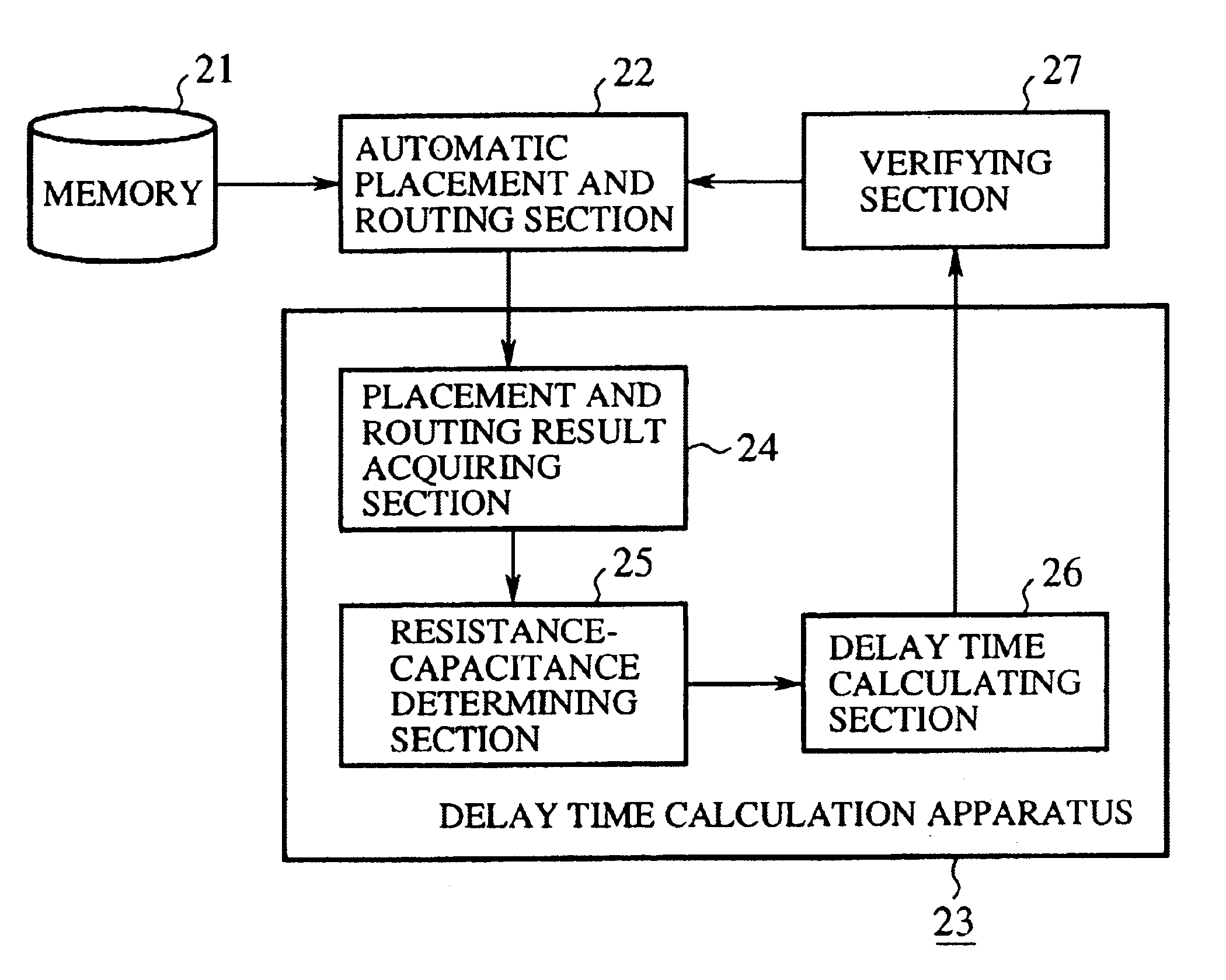
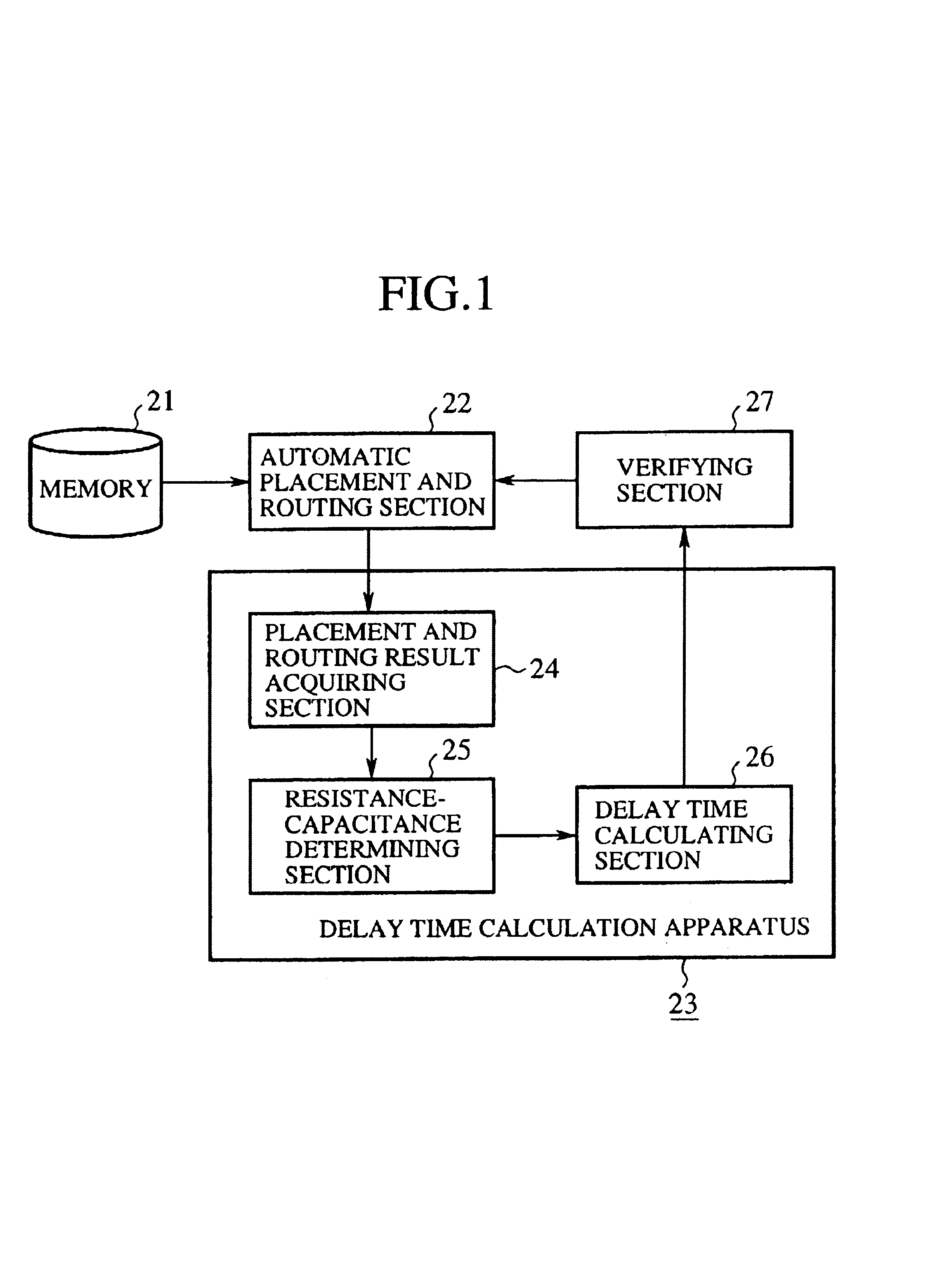
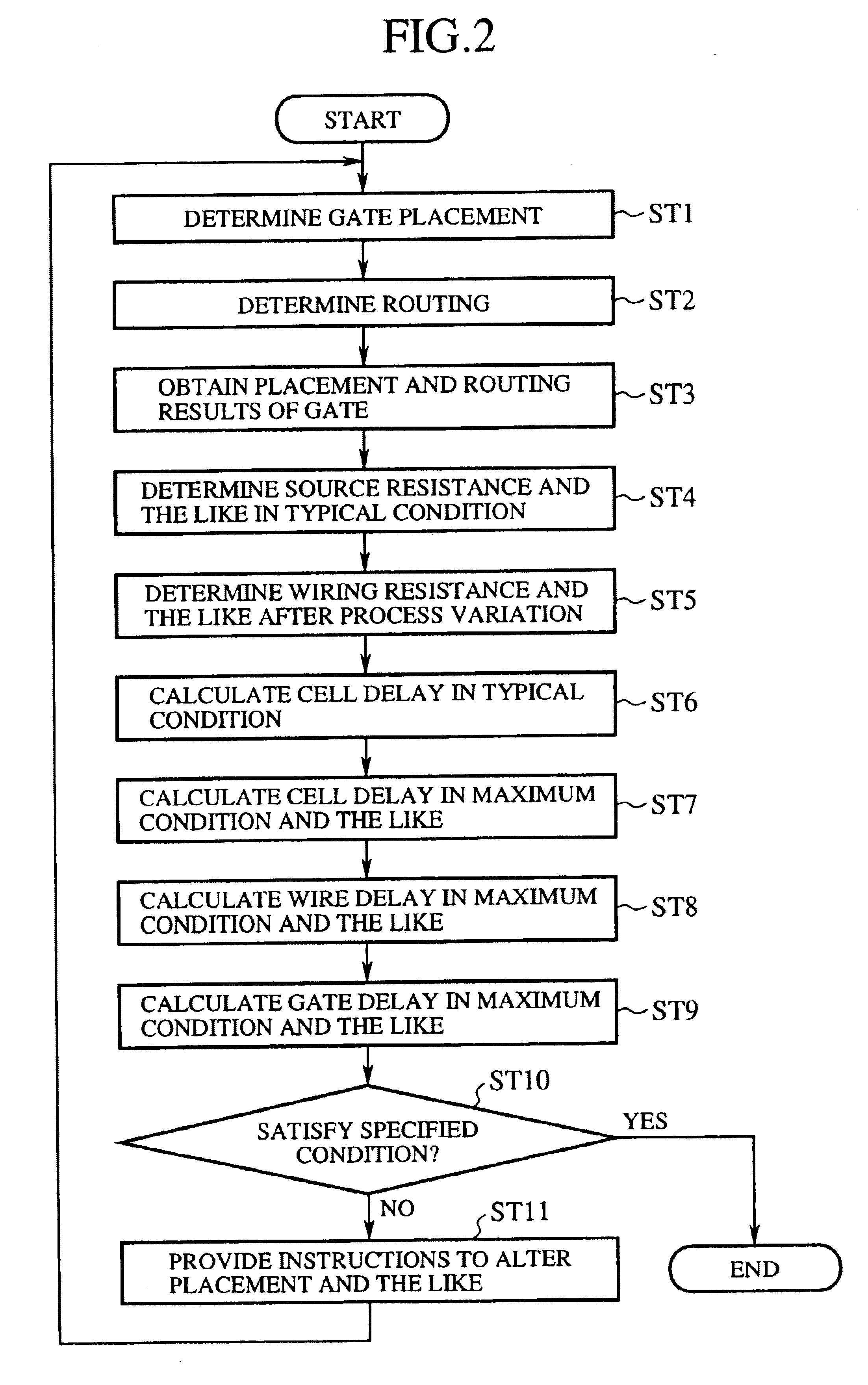
[0054]FIG. 1 is a block diagram showing a configuration of an embodiment 1 of the integrated circuit design apparatus in accordance with the present invention. In FIG. 1, the reference numeral 21 designates a memory for storing placing conditions of a plurality of gates of the semiconductor integrated circuit and routing conditions between the gates; and 22 designates an automatic placement and routing section for placing the gates considering the placing conditions stored in the memory 21, and for routing between the gates considering the routing conditions. The reference numeral 23 designates a delay time calculation apparatus for calculating gate delay time after a process variation; and 24 designates a placement and routing result acquiring section for obtaining placement results of the gates and the routing results between the gates the automatic placement and routing section 22 generates.

[0055]The reference numeral 25 designates a resistance-capacitance determining section for...

embodiment 2

[0081]Although the foregoing embodiment 1 calculates the gate delays after the process variation, they can vary with temperature because the wiring resistance R(typ) varies with temperature.

[0082]In view of this, the gate delays after the process variation can be calculated as follows using the temperature variation coefficients KTWire(max) and KTWire(min) considering the temperature variations (see, FIGS. 4 and 5).

wire_delay(max)=FWire(Rs(typ), Cd(typ), C(max), R(max))×KTWire(max)  (26)

wire_delay(min)=FWire(Rs(typ), Cd(typ), C(min), R(min))×KTWire(min)  (27)

[0083]The temperature variation coefficients KTWire(max) and KTWire(min), however, are determined considering only the variations in the wiring resistance R(typ) under the assumption that all the cells of the semiconductor integrated circuit have the same source resistance Rs(typ) and diffusion capacitance Cd(typ). Accordingly, if the source resistance Rs(typ) and diffusion capacitance Cd(typ) of the cell to which the wire is co...

embodiment 3

[0089]The foregoing embodiments 1 and 2 calculate the cell delays cell_delay(max) and cell_delay(min) in the maximum and minimum conditions by multiplying the cell delays cell_delay(typ)′ and cell_delay(typ)″ in the typical condition by the process variation coefficients KPcell(max) and KPcell(min) for the cell delay. However, since the process variation coefficients KPcell(max) and KPcell(min) for the cell delay are values common to all the cells of the semiconductor integrated circuit rather than the values proper to the target cell for the delay time calculation, they can include large errors depending on the target cell for the delay time calculation.

[0090]In view of this, to achieve the calculation of the cell delays cell_delay(max) and cell_delay(min) in the maximum and minimum conditions without using the process variation coefficients KPcell(max) and KPcell(min), the present embodiment 3 has the resistance-capacitance determining section 25 determine the source resistances R...


PUM


Abstract

A delay time calculation apparatus includes a resistance-capacitance determining section for determining a source resistance and a diffusion capacitance of a target gate of a delay time calculation before a process variation, and a wiring resistance and a wiring capacitance of a wire connected to the gate after the process variation. The delay time of the gate is calculated according to the results the resistance-capacitance determining section obtains. It can solve a problem of a conventional apparatus in that although the conventional apparatus can calculate the delay time of the gate accurately as long as the process variation coefficients for the cell delay and wire delay match the target gate of the delay time calculation, it becomes increasingly difficult to calculate the delay time accurately with an increase in the error of the process variation coefficients.

Description

BACKGROUND OF THE INVENTION[0001]1. Field of the Invention[0002]The present invention relates to a delay time calculation apparatus for calculating the delay time of a gate after a process variation and to an integrated circuit design apparatus using the same.[0003]2. Description of Related Art[0004]A semiconductor integrated circuit is composed of a plurality of gates. A delay time of each gate (called “gate_delay” from now on) is defined as a sum of a delay time occurring within the gate (called “cell_delay” from now on) and a delay time (called “wire_delay” from now on) occurring in wire connected to the gate.[0005]FIG. 10 is a schematic diagram illustrating a gate delay gate_delay(typ) in a typical condition, in which the delay time is typical (see, expression (1)); FIG. 11 is a schematic diagram illustrating a gate delay gate_delay(max) in a maximum condition, in which the cell delay is maximum (see, expression (2)); and FIG. 12 is a schematic diagram illustrating a gate delay ...

Claims


Application Information

Patent Timeline
Patent Type & Authority Patents(United States)
IPC IPC(8): G06F17/50H01L21/82
CPCG06F17/5036G06F17/5031G06F30/3312G06F30/367
Inventor SAKANO, MIHO
Owner RENESAS TECH CORP
Why Eureka
Try Eureka