

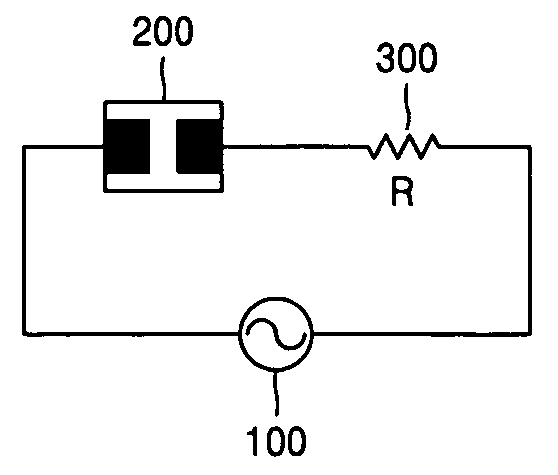
Current-jump-control circuit including abrupt metal-insulator phase transition device
a phase transition device and current control technology, which is applied in the direction of electrical equipment, emergency protective arrangements for limiting excess voltage/current, and devices that cannot endure against large currents, devices may fail, and abrupt metal-insulator phase transition may generate a large amount of current (current jump) abruptly
- Summary
- Abstract
- Description
- Claims
- Application Information
AI Technical Summary
Benefits of technology
Problems solved by technology
Method used
Image

Examples
first embodiment
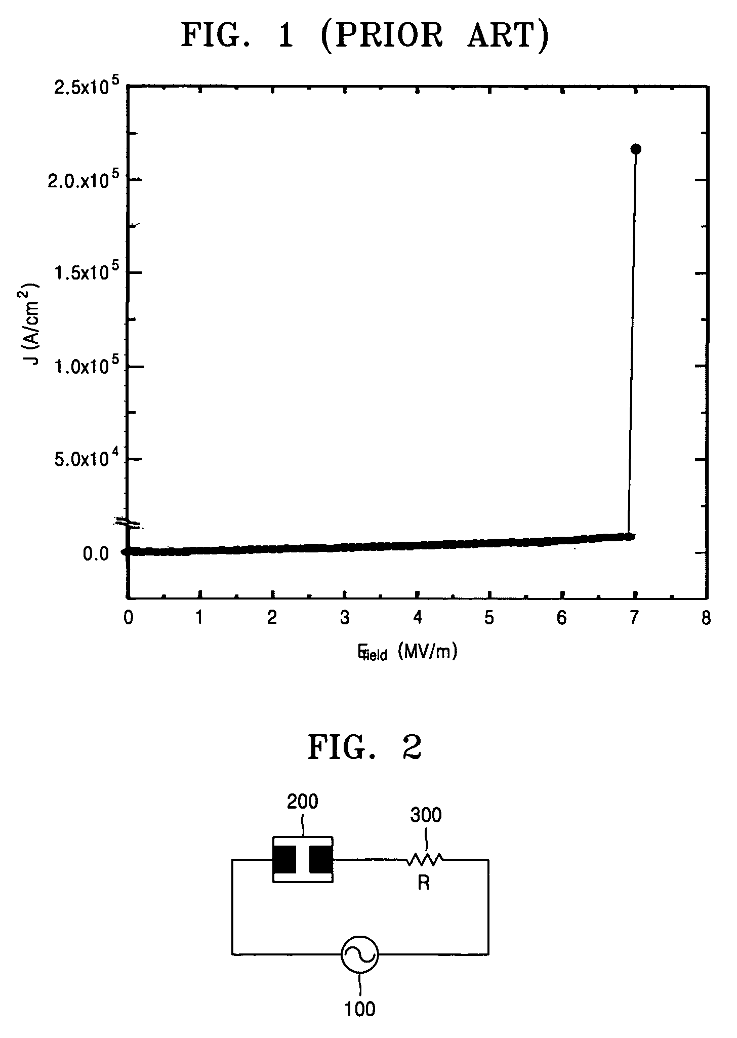
[0027]FIG. 4 is a graph showing the resistance dependence of the current jump of voltage-current density characteristic of a current control circuit including an abrupt metal-insulator phase transition device according to the present invention. In FIG. 4, a horizontal axis represents a voltage (V) applied between the first electrode 230 and the second electrode 240, and a vertical axis is a current density (J) between the first electrode 230 and the second electrode 240.
[0028]The abrupt metal-insulator phase transition device 200 used in the test of FIG. 4 is a device having the sapphire (Al2O3) substrate 210 and the vanadium dioxide (VO2) insulator 220, and has a channel length of 5 μm between the first electrode 230 and the second electrode 240 and a channel width of 25 μm. In FIG. 4, a line indicated by a reference symbol ‘●’ corresponds to a case that the resistance (R) of the resistive element 300 is 1.0 kΩ, a line indicated by a reference symbol ‘▴’ corresponds to a case that ...
second embodiment
[0029]FIG. 5 is a graph showing the resistance dependence of the current jump of voltage-current density characteristic of a current control circuit including an abrupt metal-insulator phase transition device according to the present invention. In FIG. 5, a horizontal axis represents a voltage (V) applied between the first electrode 230 and the second electrode 240, and a vertical axis is a current density (J) between the first electrode 230 and the second electrode 240.
[0030]The abrupt metal-insulator phase transition device 200 used in the test of FIG. 5 is a device using the silicon (Si) substrate 210 and the vanadium dioxide (VO2) insulator 220, and has a channel length of 5 μm between the first electrode 230 and the second electrode 240 and a channel width of 25 μm. In FIG. 5, a line indicated by a reference symbol ‘▪’ corresponds to a case that the resistance (R) of the resistive element 300 is 110 Ω, a line indicated by a reference symbol ‘●’ corresponds to a case that the re...
PUM
 Abstract
Description
Claims
Application Information