Optical AND gate and waveform shaping device

a waveform shaping and optical gate technology, applied in the direction of logic circuits, pulse techniques, instruments using specific components, etc., can solve the problems of signal-to-noise ratio, transmission limit, transmission distance limit, etc., and achieve the effect of easy-to-convert wavelength

Inactive Publication Date: 2006-01-17
FUJITSU LTD
View PDF4 Cites 43 Cited by
  • Summary
  • Abstract
  • Description
  • Claims
  • Application Information

AI Technical Summary

Benefits of technology

[0016]It is therefore an object of the present invention to provide a method and device which can easily-convert the wavelength of signal light int...

Problems solved by technology

In this kind of optical amplifier, amplified spontaneous emission (ASE) noise generated in association with the amplification is added to cause a reduction in signal-to-noise ratio (S/N ratio), so that the number of repeaters is limited to result in the limit of a transmission distance.
Further, waveform degradation due to the chromatic dispersion owned by an optical fiber and the nonlinear optical effects in the fiber is another cause of the transmission limit.
However, since the performance of this device depends on t...

Method used


Image

  • Optical AND gate and waveform shaping device
  • Optical AND gate and waveform shaping device
  • Optical AND gate and waveform shaping device

Examples


Embodiment Construction

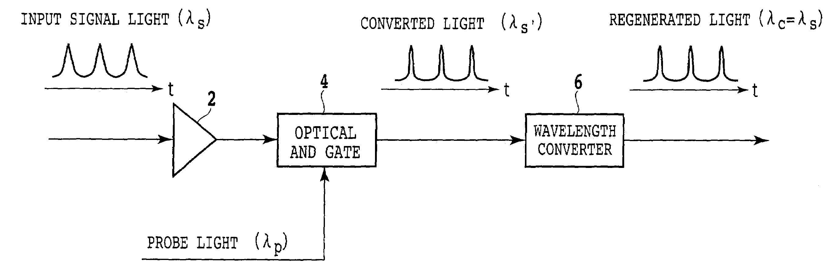
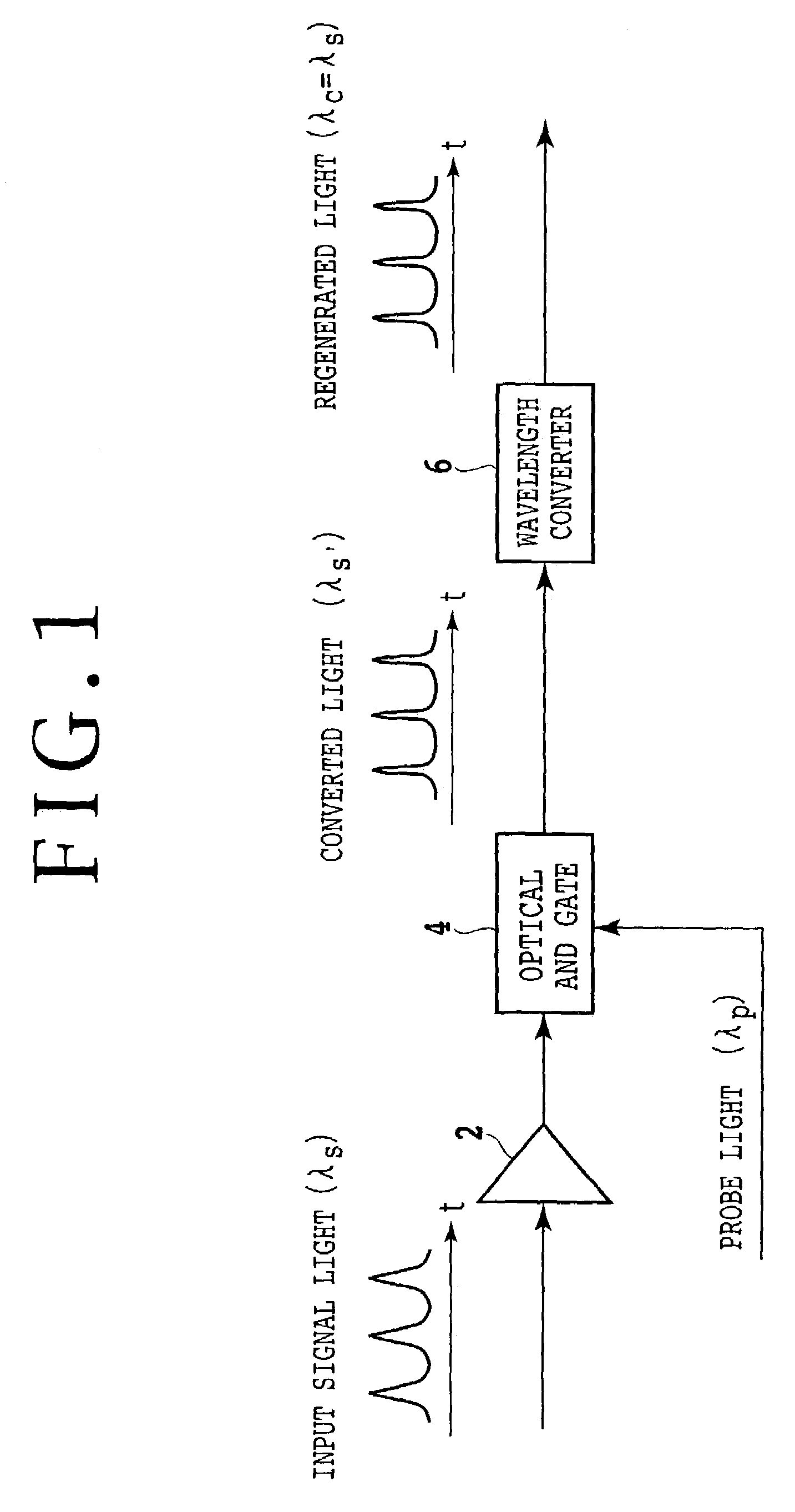
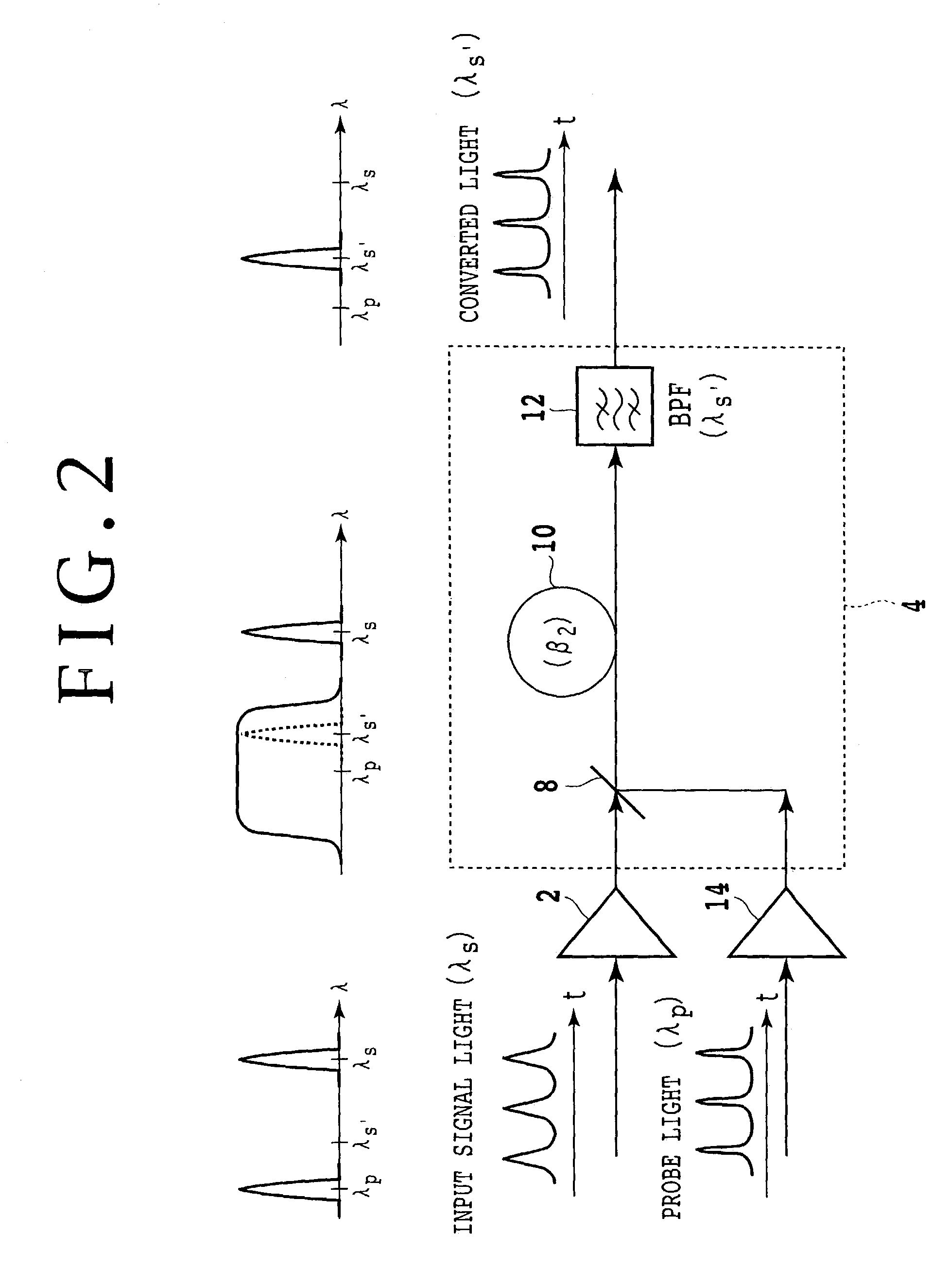
[0037]Some preferred embodiments of the present invention will now be described in detail with reference to the attached drawings. Throughout the drawings, substantially the same or like parts are denoted by the same reference numerals.

[0038]In a preferred embodiment of the present invention, probe light is subjected to cross phase modulation (XPM) by signal light in an optical AND gate to thereby broaden the spectrum of the probe light, and a component different from the center wavelength of the spectrum is extracted from the broadened spectrum by an optical bandpass filter to thereby extract a wavelength converted signal component.

[0039]For example, the wavelength converted signal component is further subjected to wavelength conversion to thereby make the wavelength of the wavelength converted signal component equal to the wavelength of the original signal light or to any arbitrary wavelength. This wavelength conversion may be effected by broadening the spectrum by self phase modu...


PUM


Abstract

The method according to the present invention includes the steps of inputting an optical signal having a first wavelength and probe light having a second wavelength different from the first wavelength into a nonlinear optical medium, broadening the spectrum of the probe light through cross phase modulation between the optical signal and the probe light inside the nonlinear optical medium, and extracting a signal component including a modulated component of the optical signal and having a band narrower than the band of the spectrum broadened. According to the present invention it can be possible to provide a method and device which can easily convert the wavelength of signal light into an arbitrary wavelength in performing optical 3R functions.

Description

BACKGROUND OF THE INVENTION[0001]1. Field of the Invention[0002]The present invention relates to a method and device for waveform-shaping signal light, and more particularly to an optical AND gate for performing optical signal regeneration by an optical signal and an optical clock.[0003]2. Description of the Related Art[0004]In an optical fiber communication system that has been put to practical use in recent years, a reduction in signal power due to transmission line loss, coupling loss, etc. is compensated by using an optical amplifier such as an erbium doped fiber amplifier (EDFA). The optical amplifier is an analog amplifier, which functions to linearly amplify a signal. In this kind of optical amplifier, amplified spontaneous emission (ASE) noise generated in association with the amplification is added to cause a reduction in signal-to-noise ratio (S / N ratio), so that the number of repeaters is limited to result in the limit of a transmission distance. Further, waveform degrada...

Claims


Application Information

Patent Timeline
IPC IPC(8): G02F1/365G02F2/02G02F3/00G02F1/35G02F2/00
CPCG02F1/3515H04B10/299G02F2/004G02F3/00
Inventor WATANABE, SHIGEKI
Owner FUJITSU LTD
Why Eureka
Try Eureka