Method and apparatus for precision measurement of film thickness

a technology of precision measurement and film thickness, applied in the direction of instruments, resistance/reactance/impedence, corona discharge, etc., can solve the problems of inconvenient use, inconvenient use, and the most expensive instrument of this type compared to metrological equipment of other systems, and achieve high-accuracy, contactless measurement, and simple

Inactive Publication Date: 2006-01-24
MULTIMETRIXS
View PDF11 Cites 58 Cited by
  • Summary
  • Abstract
  • Description
  • Claims
  • Application Information

AI Technical Summary

Benefits of technology

[0033]It is an object of the present invention to provide a method and apparatus for inexpensive, simple, high-accurate and efficient contactless measurement of film thicknesses below 1000 Angstroms by means of a microwave resonance sensor.

Problems solved by technology

A disadvantage of radiation methods is the use of X-ray or gamma radiation that requires special safety measures for protection of the users against the radiation.
The instruments of this type are the most expensive as compared to metrological equipment of other systems.
Although the optical interferometry method produces the most accurate results in measuring the thickness of a coating film, it has a limitation.
In other words, this method is unsuitable or is difficult to use for measuring conductive films thicker than 200 Å to 500 Å.
Therefore, this method is inapplicable to measuring thickness of the film that has been already deposited.
However, the four-point method has some disadvantages.
The main problem associated with the aforementioned four-point probe method is that in each measurement it is required to ensure reliable contact in each measurement point.
This is difficult to achieve since conditions of contact vary from sample to sample as well as between the four pointed contact elements of the probe itself in repeated measurement with the same probe.
Such non-uniformity affects the results of measurements and makes it impossible to perform precision calibration.
This condition is unacceptable for measuring thickness of a thin film with microscopic thickness, which moves relative to the sensor, e.g., for mapping, i.e., for determining deviations of the thickness over the substrate.
In his important work, S. Roach generalized the relationships between the aforementioned parameters and showed that, irrespective of actual dimensions of the sensor, “the rapid loss of sensitivity with distance strictly limits the range of eddy current sensor to about ½ the coil diameter and constitutes the most important limitation of this type of sensing”.
It is understood that conventional inductive sensors of the types described above and used in a conventional manner are inapplicable for the solution of the above problem.
The distance between the measurement element of the inductive sensor and the surface of the film being measured also becomes a critical issue.
However, the sensor disclosed in the aforementioned patent application could not completely solve the problems associated with accurate measurement of super-thin films, e.g., of those thinner than 500 Angstroms.
This is because the construction of the aforementioned sensor is limited with regard to the range of operation frequencies, i.e., the sensor cannot be use in frequencies exceeding 30 MHz.
Furthermore, the aforementioned sensor requires the use of a complicated distance-stabilization system.
The above problems restrict practical application of the method and apparatus of U.S. patent application Ser. No. 09 / 954,550 for measuring thickness of very thin films and deviations from the thickness in the aforementioned films.
Furthermore, it is obvious that the aforementioned method and apparatus do not allow thickness measurement of non-conductive films.
Another disadvantage of the sensor of the aforementioned application is that it is very sensitive to the distance between the sensor and the film.
This requirement dictates the use of expensive and complicated distance-measurement means such as microinterferometers or microscopes.

Method used


Image

  • Method and apparatus for precision measurement of film thickness
  • Method and apparatus for precision measurement of film thickness
  • Method and apparatus for precision measurement of film thickness

Examples


Embodiment Construction

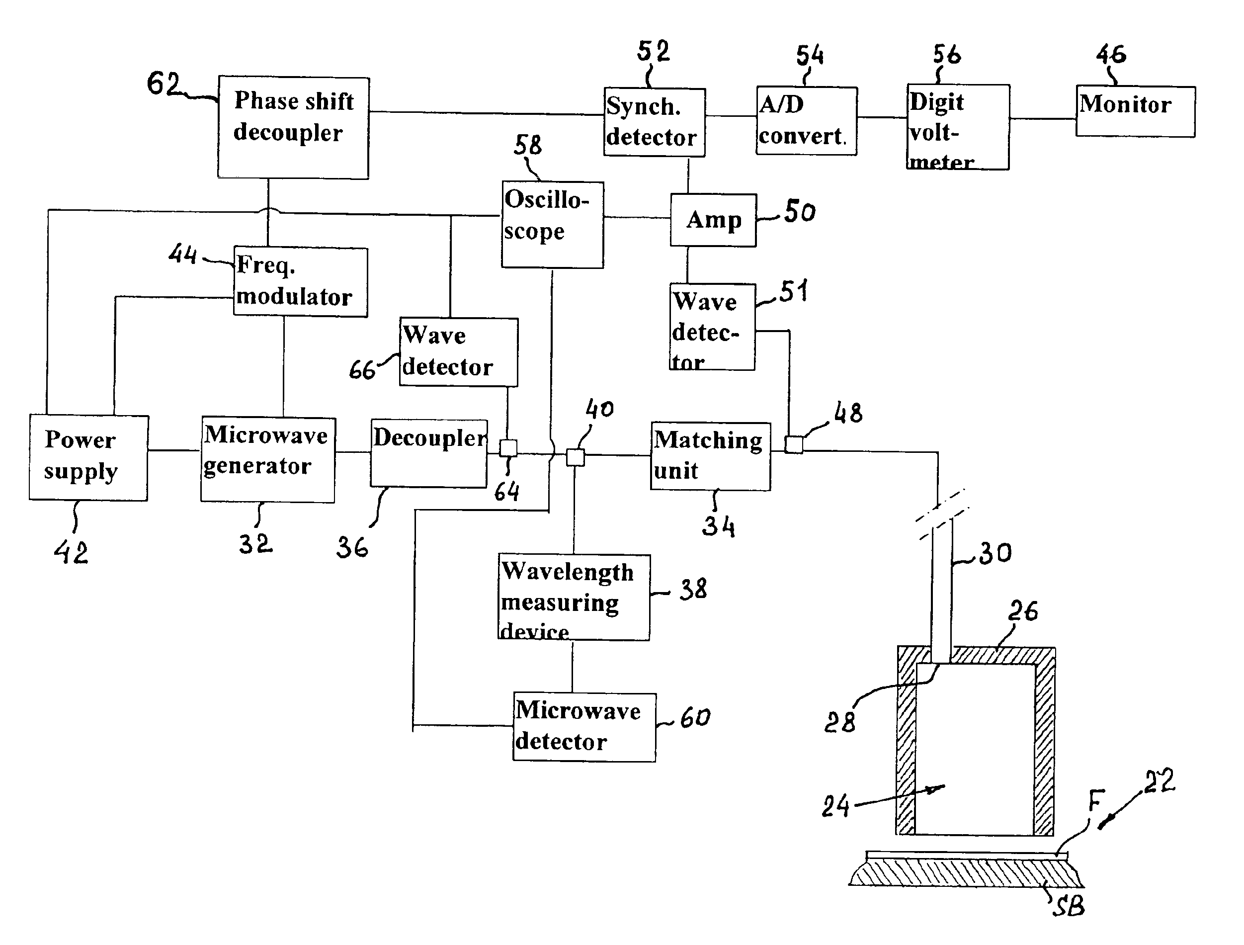
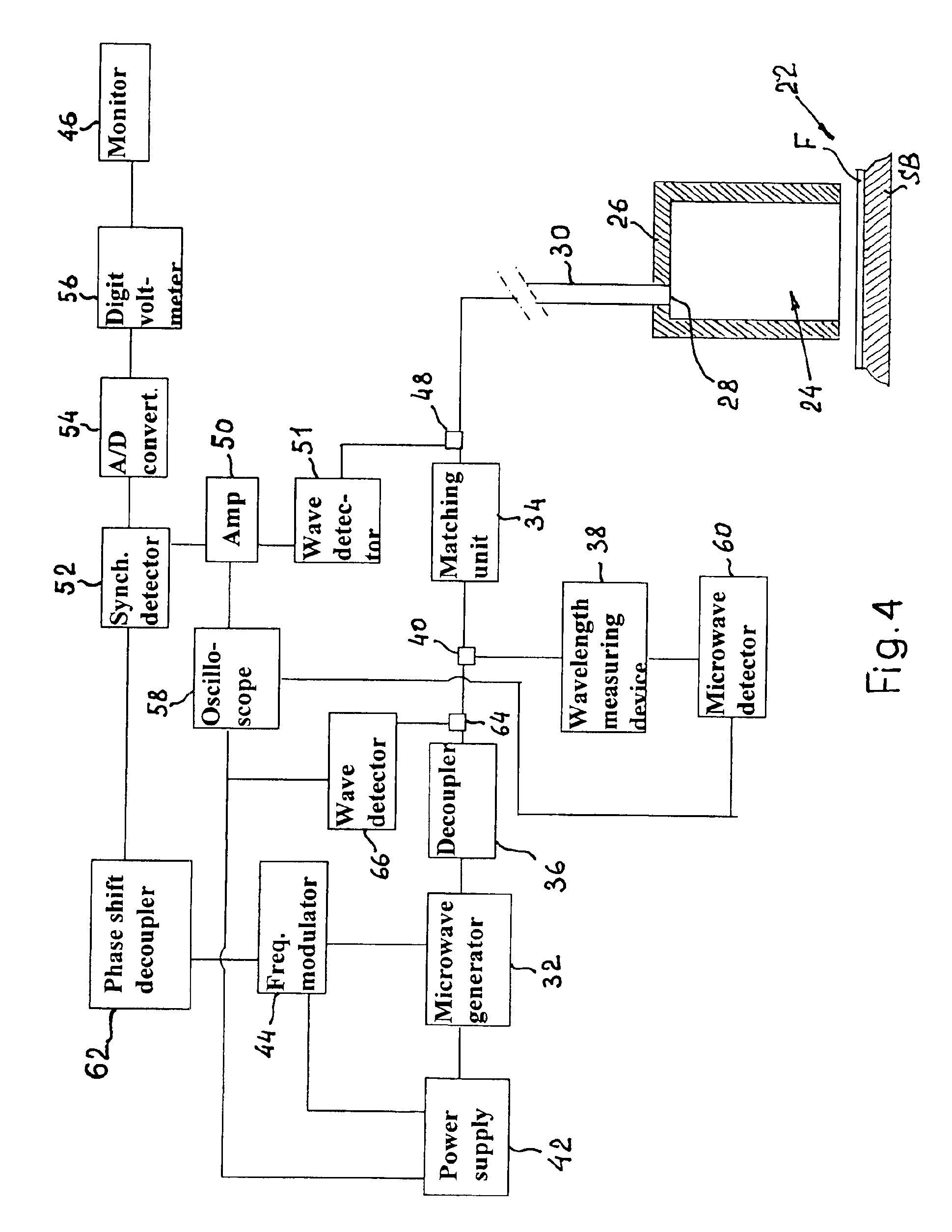
[0049]The apparatus, which as a whole is designated by reference numeral 20, will be described in general in order to show main components and their interconnections, and then the main units will be described separately in more detail. It should be understood that the specific components and their arrangement shown in FIG. 4 represent only one possible example of the apparatus, which can be embodied in a variety of other acceptable modifications.

[0050]The main unit or heart of the apparatus is a cylindrical microwave resonator unit 22 which functions as a film-thickness sensor unit for measuring the thickness of a conductive thin film F placed on a non-conductive substrate SB. The resonator unit 22 comprises a cylindrical body, which has one end 24 (which faces the film F) open in a non-working state of the resonator and another end covered by a membrane 26 with an opening 28 for connection of one end of a microwaveguide line30. The opposite end of the microwaveguide line 30 is conn...


PUM


Abstract

An apparatus for measuring thickness in super-thin films consists of a special resonator unit in the form of an open-bottom cylinder which is connected to a microwave swept frequency microwave source via a decoupler and a matching unit installed in a waveguide that connects the resonator unit with the microwave source. The apparatus operates on the principle that thin metal film F, the thickness of which is to be measured, does not contact the end face of the open bottom of the cylindrical resonator sensor unit and functions as a bottom of the cylindrical body. The design of the resonator excludes generation of modes other than the resonance mode and provides the highest possible Q-factor. As the conductivity directly related to the film thickness, it is understood that measurement of the film thickness is reduced to measurement of the resonance peak amplitudes. This means that superhigh accuracy inherent in measurement of the resonance peaks is directly applicable to the measurement of the film thickness or film thickness deviations.

Description

FIELD OF THE INVENTION[0001]The present invention relates to the field of measurement of film thickness, more specifically, to measuring thickness of conductive films on various conductive substrates. In particular, the invention may find use in measuring thickness of coating films on semiconductor wafers, hard-drive disks, or the like.BACKGROUND OF THE INVENTION[0002]There exists a great variety of methods and apparatuses used in the industry for measuring thickness of coating films and layers applied or laid onto substrates. These methods and apparatuses can be classified in accordance with different criteria. Classification of one type divides these methods into direct and indirect.[0003]An example of the direct method is measurement of a thickness in thin metal coating films by means of so-called X-ray reflectivity. One of these methods is based on a principle that X-rays and gamma rays are absorbed by matter. When a beam of rays passes through a material, the amount of the beam...

Claims


Application Information

Patent Timeline
Patent Type & Authority Patents(United States)
IPC IPC(8): G01R27/32G01B15/02
CPCG01B15/02
Inventor KESIL, BORISVELIKOV, LEONIDVOROBYEV, YURI
Owner MULTIMETRIXS
Why Eureka
Try Eureka