Variable stage ratio buffer insertion for noise optimization in a logic network

Inactive Publication Date: 2006-01-24
CADENCE DESIGN SYST INC
View PDF7 Cites 6 Cited by
  • Summary
  • Abstract
  • Description
  • Claims
  • Application Information

AI Technical Summary

Problems solved by technology

With the continued scaling of process technology, however, unwanted capacitive coupling of signals between adjacent interconnect wires on an integrated circuit becomes a very real problem.
The occurrence of crosstalk on certain operations can cause a chip to malfunction, for example, when a noise glitch is induced on a metal line as a consequence of a

Method used


Image

  • Variable stage ratio buffer insertion for noise optimization in a logic network
  • Variable stage ratio buffer insertion for noise optimization in a logic network
  • Variable stage ratio buffer insertion for noise optimization in a logic network

Examples


Embodiment Construction

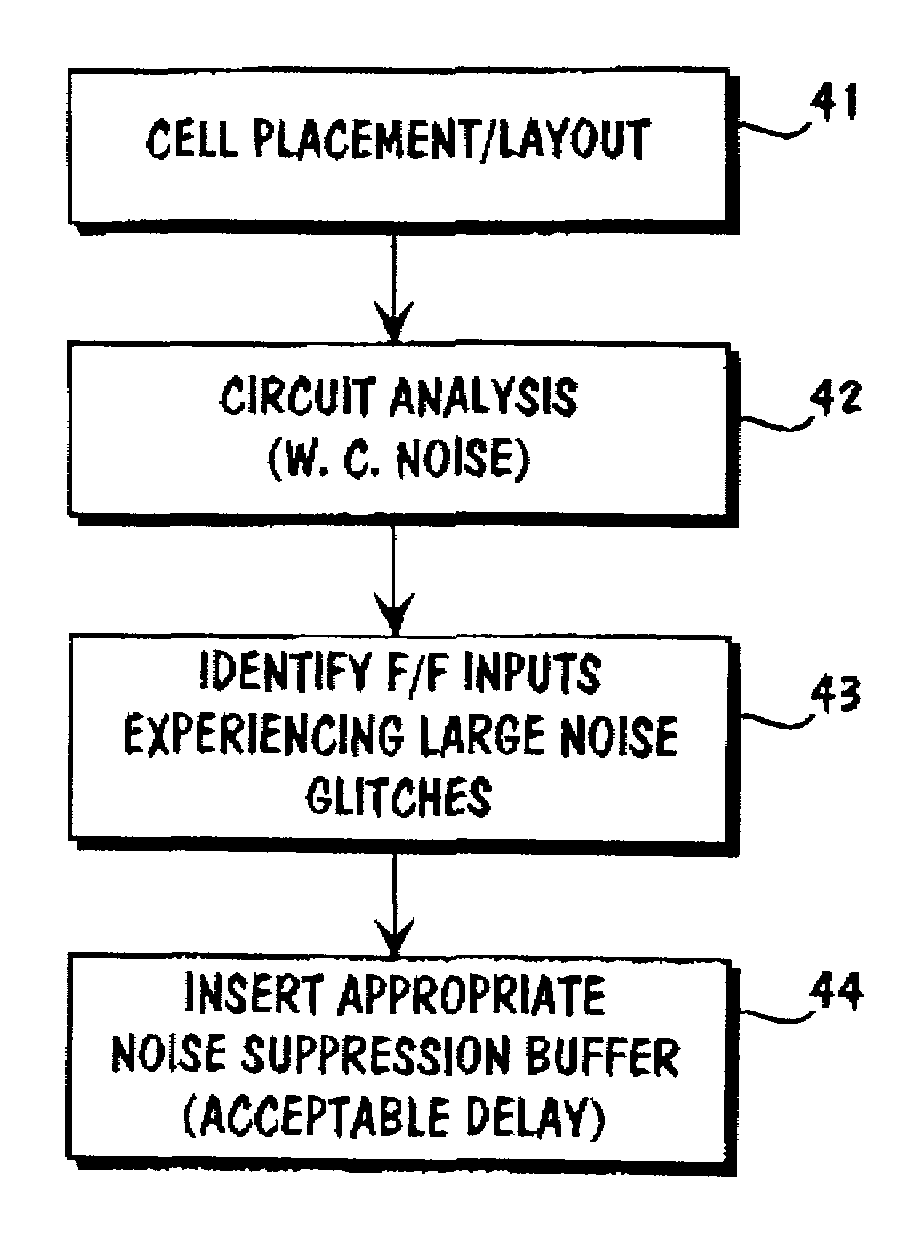
[0014]A variable stage ratio buffer for insertion in a logic network is described. In the following description, specific details are set forth, such as device types, sizes, voltage levels, etc., in order to provide a thorough understanding of the present invention. Practitioners having ordinary skill in the semiconductor arts will understand that the invention may be practiced without many of these details. In other instances, well-known elements, device structures, and processing steps have not been described in detail to avoid obscuring the invention.

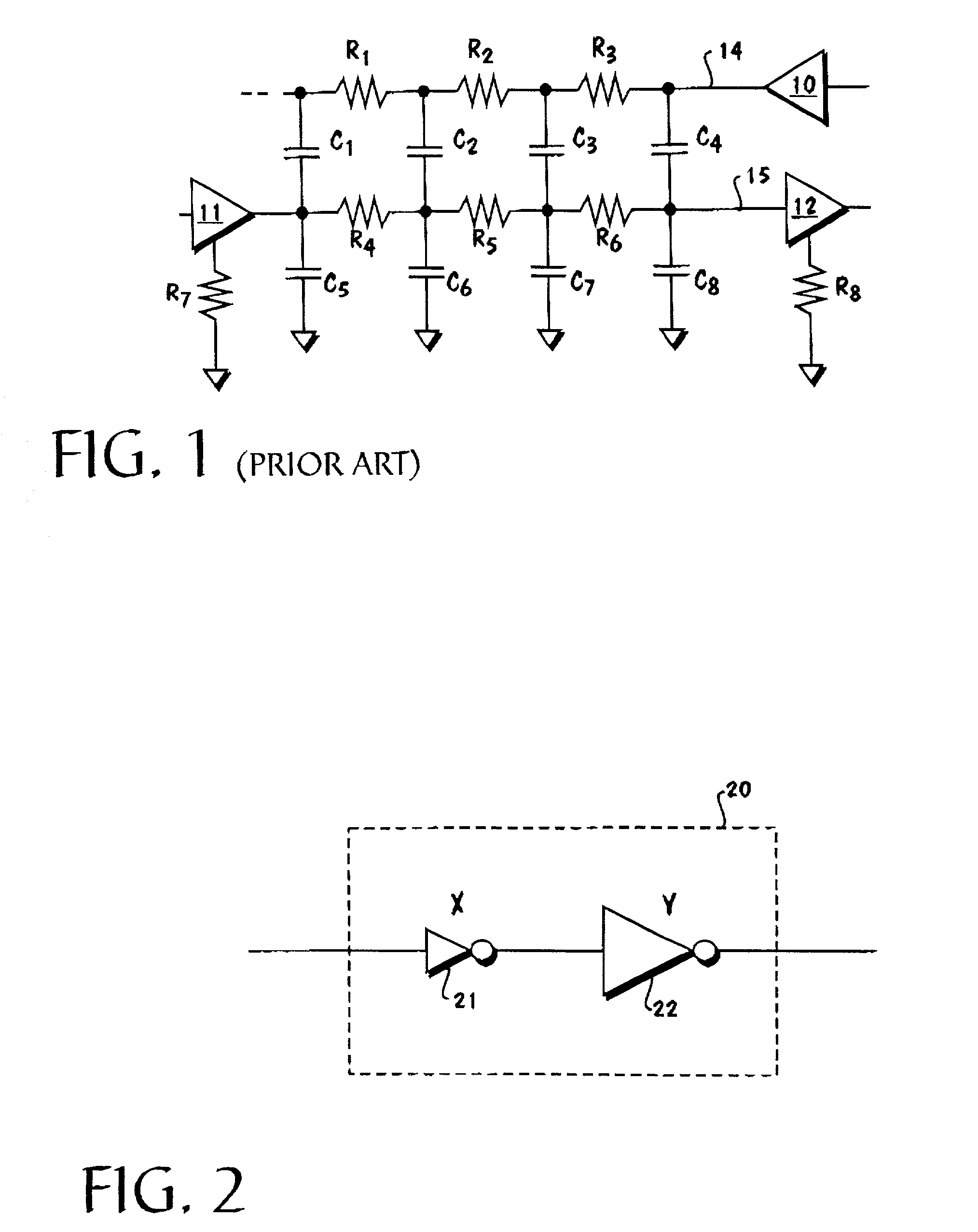
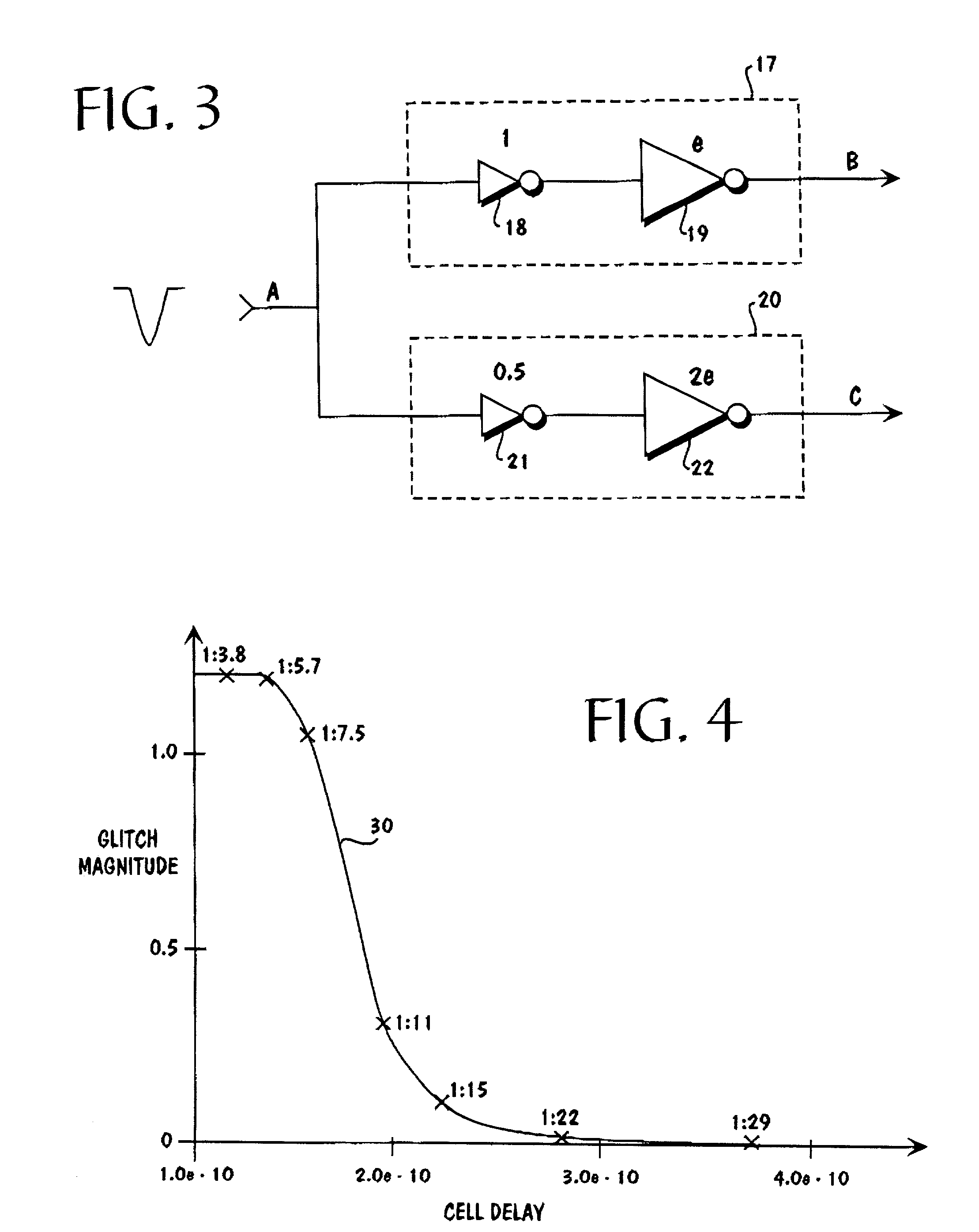
[0015]FIG. 2 is a logic diagram of a variable stage ratio buffer 20 for use in optimizing noise rejection in an integrated circuit. Buffer 20 comprises a pair of inverters 21 and 22 coupled in series. In one embodiment, each of the inverters are fabricated utilizing conventional complementary metal-oxide semiconductor (CMOS) transistor devices. Other fabrication technologies using different types of devices may also be used.

[0016]Inv...


PUM


Abstract

A buffer for use in a logic circuit comprises input and output nodes. A first inverter having a first device size is coupled to the input node. A second inverter is coupled in series with the first inverter and with the output node. The second inverter having a second device size at least six times greater than the first device size. It is emphasized that this abstract is provided to comply with the rules requiring an abstract that will allow a searcher or other reader to quickly ascertain the subject matter of the technical disclosure. It is submitted with the understanding that it will not be used to interpret or limit the scope or meaning of the claims. 37 CFR 1.72(b).

Description

FIELD OF THE INVENTION[0001]The present invention relates to the design of integrated circuits. More specifically, the present invention relates to buffers for use in logic networks.BACKGROUND OF THE INVENTION[0002]Optimization of delay in global interconnect paths has long been a goal in the design of integrated circuits. A number of algorithms and design techniques have been used to optimize delay and timing slack in designs utilizing submicron device fabrication technologies. With the continued scaling of process technology, however, unwanted capacitive coupling of signals between adjacent interconnect wires on an integrated circuit becomes a very real problem. This phenomenon is referred to as crosstalk. The occurrence of crosstalk on certain operations can cause a chip to malfunction, for example, when a noise glitch is induced on a metal line as a consequence of a fast switching operation on a nearby line.[0003]FIG. 1 shows an analog model for internally induced crosstalk nois...

Claims


Application Information

Patent Timeline
IPC IPC(8): G06F17/50H03K19/003
CPCH03K19/00361G06F17/505G06F30/327
Inventor TSENG, KENNETH HING KEY
Owner CADENCE DESIGN SYST INC
Why Eureka
Try Eureka