
Bistable nematic liquid crystal device

a liquid crystal device and nematic technology, applied in liquid crystal compositions, instruments, chemistry apparatus and processes, etc., can solve the problems of complex matrix addressing of displays, added manufacturing costs, and difficult manufacturing of large area tft arrays, so as to improve the switching and improve the switching of devices

Inactive Publication Date: 2006-01-31
HEWLETT PACKARD DEV CO LP
View PDF37 Cites 8 Cited by
  • Summary
  • Abstract
  • Description
  • Claims
  • Application Information

AI Technical Summary

Benefits of technology

The present invention provides a bistable liquid crystal display device with a layer of nematic liquid crystal material enclosed by two cell walls. The device includes electrodes for applying an electric field across the liquid crystal material. An alignment layer is present on the inner surface of at least one of the cell walls, which induces a planar or tilted alignment of the liquid crystal molecules. The device has a fast bistable switching speed, with voltage pulses of around 50 μs duration being sufficient to cause switching. The orientation of the director is induced by the geometry of the holes, rather than by the regular lattice or the alignment layer. The holes may have straight or tilted sides, or curved or irregular surfaces. The alignment layer may be continuous or discontinuous, and it may be formed from a dielectric material or metal. The device may also have twist induced in the liquid crystal material, which improves the optical characteristics of the device. The invention provides a robust display device with a unique alignment mechanism that induces a desired alignment of the liquid crystal molecules.

Problems solved by technology

Each “on” pixel must be maintained above an electric field threshold, which can cause problems in the matrix addressing of complex displays.
These problems can be overcome by driving each pixel by a thin film transistor (TFT), but manufacturing large area TFT arrays is difficult and adds to manufacturing costs.

Method used


Image

  • Bistable nematic liquid crystal device
  • Bistable nematic liquid crystal device
  • Bistable nematic liquid crystal device

Examples


Embodiment Construction

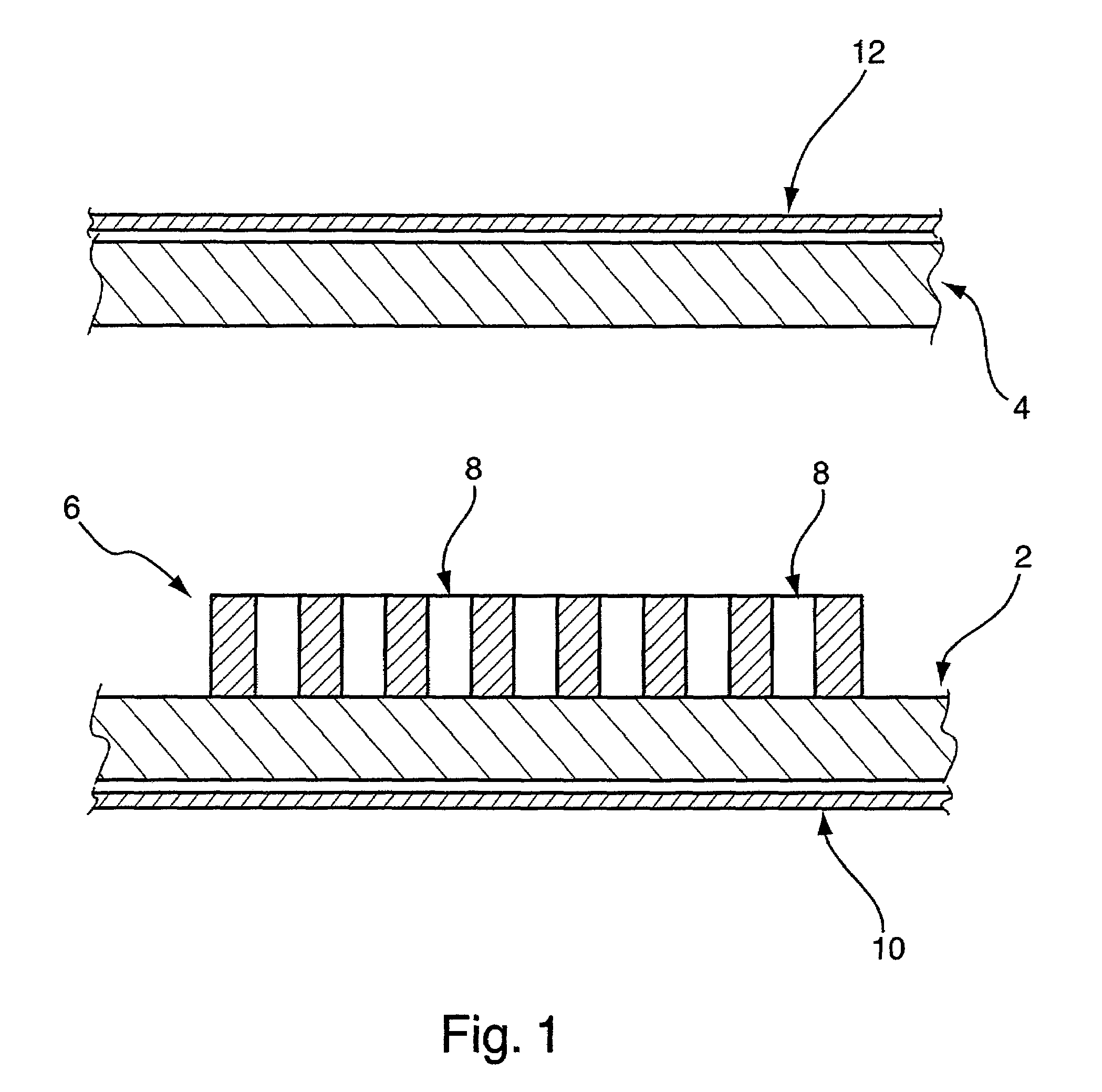
[0046]The bistable nematic cell shown schematically in FIG. 1 comprises a first cell wall 2 and a second cell wall 4 which enclose a layer of nematic LC material of negative dielectric anisotropy. The inner surface of each cell wall is provided with a transparent electrode pattern (not shown), for example row electrodes on the first cell wall 2 and column electrodes on the second cell wall 4, in a known manner.

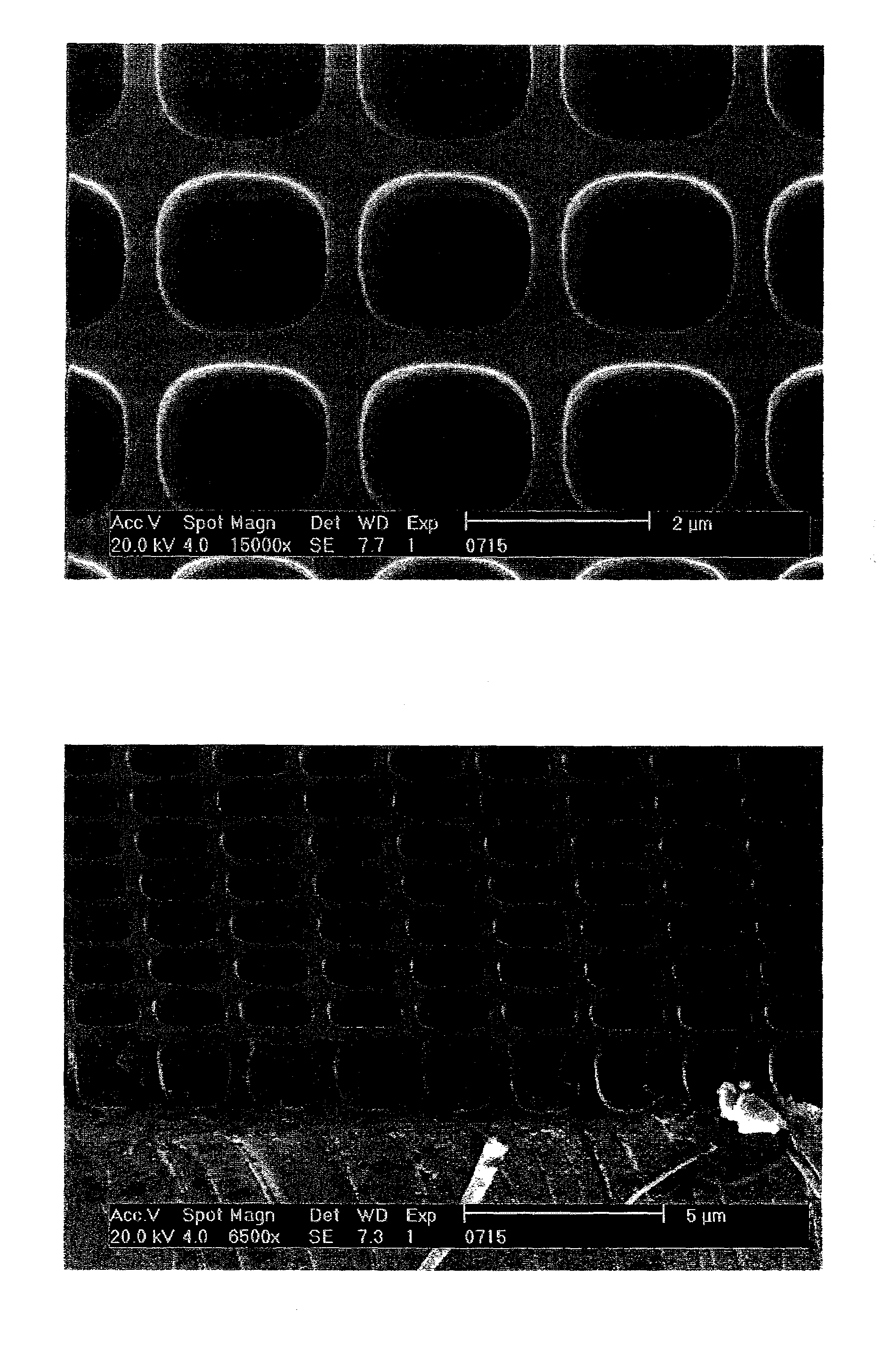
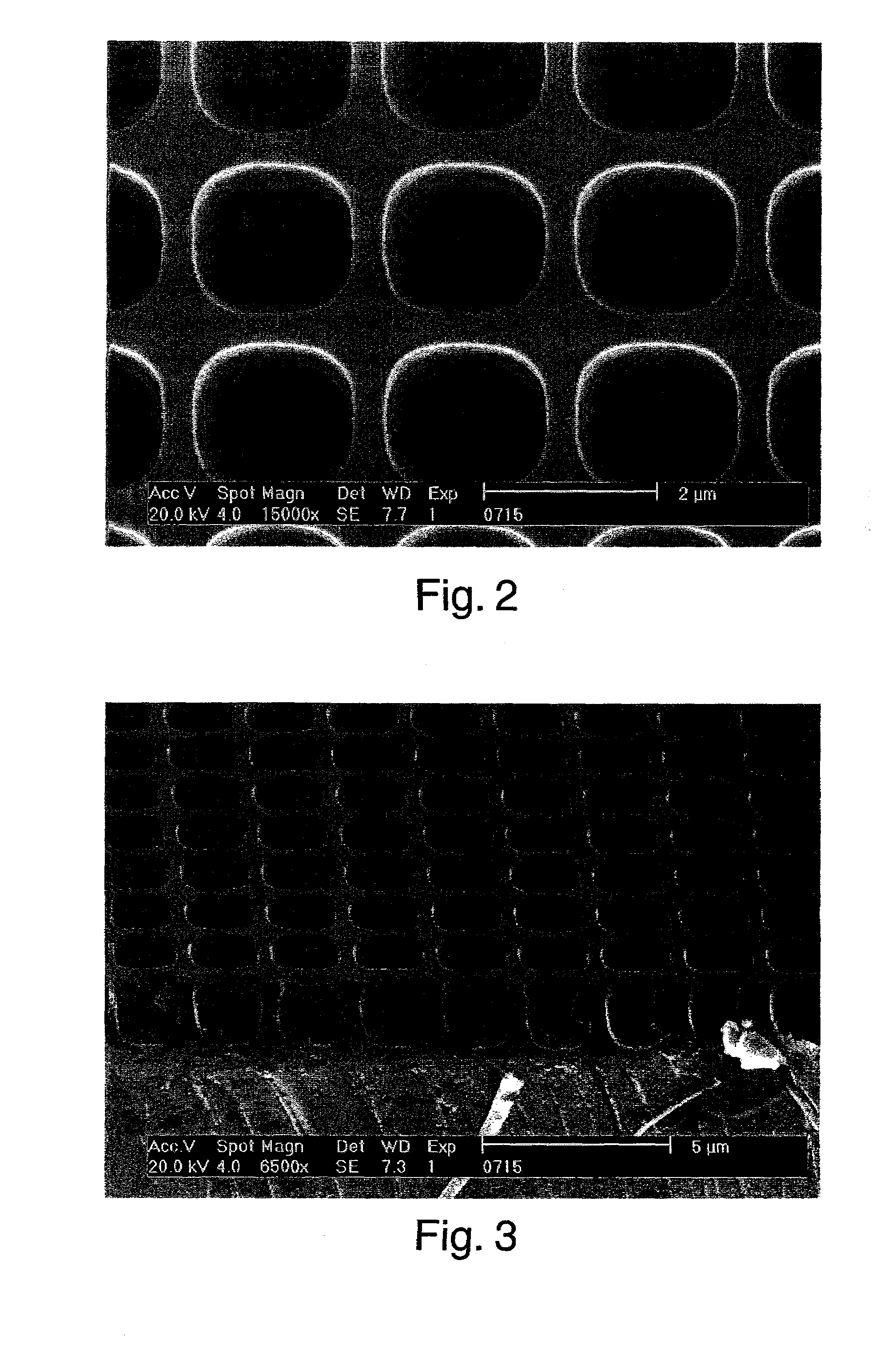
[0047]The inner surface of the first cell wall 2 is provided with a layer 6 of a dielectric material in which is formed a regular array of square holes 8, and the inner surface of the second cell wall 4 is flat. The holes 8 are approximately 1 μm deep and the cell gap (wall to wall) is typically 2 to 4 μm. The flat surface is treated to give homeotropic alignment. The holes 8 and alignment layer 6 are not homeotropically treated. The chemical nature of the surface is such that the LC adopts a substantially planar alignment adjacent to the surface. SEM photomicrographs of an ex...


PUM

PropertyMeasurementUnit
depthaaaaaaaaaa
depthaaaaaaaaaa
widthaaaaaaaaaa

Abstract

A bistable nematic liquid crystal device includes an array of holes (8) in an alignment layer (6) on at least one cell wall (2). The alignment layer (6) induces a substantially planar local alignment of liquid crystal molecules. The holes (8) have a shape and / or orientation to induce the liquid crystal director adjacent the holes (8) to adopt two different tilt angles in substantially the same azimuthal direction. The arrangement is such that two stable liquid crystal molecular configurations can exist after suitable electrical signals have been applied to the electrodes.

Description

FIELD OF THE INVENTION[0001]This invention relates to bistable nematic liquid crystal devices.BACKGROUND OF THE INVENTION[0002]Liquid crystal devices typically comprise a pair of opposed, spaced-apart translucent cell walls with liquid crystal (“LC”) material between them. The cell walls have transparent electrode patterns for applying fields to align the LC material.[0003]LC materials are rod-like or lath-like molecules which have different optical properties along their long and short axes. The molecules exhibit some long range order so that locally they tend to adopt similar orientations to their neighbours. The local orientation of the long axes of the molecules is referred to as the director. When the director is orientated perpendicular to the plane of the cell walls, this is referred to as homeotropic alignment. Alignment of the director along the plane of the cell walls or at an angle to the plane of the cell walls is referred to respectively as planar homogeneous and tilted...

Claims


Application Information

Patent Timeline
Patent Type & Authority Patents(United States)
IPC IPC(8): G02F1/1337C09K19/02G02F1/139
CPCG02F1/133753G02F1/1391G02F1/13378G02F2001/133776G02F2001/133761G02F1/133761G02F1/133776
Inventor KITSON, STEPHEN CHRISTOPHERGEISOW, ADRIAN DEREKRUDIN, JOHN CHRISTOPHER
Owner HEWLETT PACKARD DEV CO LP
Learn More