Semiconductor package with circuit side polymer layer and wafer level fabrication method

a technology of semiconductor packaging and polymer layer, applied in the direction of semiconductor/solid-state device details, semiconductor devices, electrical devices, etc., can solve the problem of stress defects often developing in the di

Inactive Publication Date: 2006-02-07
MICRON TECH INC
View PDF36 Cites 30 Cited by
  • Summary
  • Abstract
  • Description
  • Claims
  • Application Information

AI Technical Summary

Benefits of technology

[0012]In a first embodiment, the package has a board on chip (BOC) configuration. The package includes a BOC substrate having a pattern of conductors, a semiconductor die attached to the BOC substrate and wire bonded to the conductors, and a die encapsulant encapsulating the die and the substrate. The die includes die contacts, such as bond pads or redistribution contacts on a circuit side thereof, in electrical communication with integrated circuits on the die. The die also includes planarized wire bonding contacts on the die contacts, and a planarized polymer layer encapsulating the wire bonding contacts. The planarized polymer layer prevents physical contact between the die encapsulant and the integrated circuits on the circuit side of the die, and functions as a stress defect barrier between the integrated circuits and fillers contained in the die encapsulant.
[0013]In a second embodiment, a chip on board (COB) package includes a die having a planarized polymer layer and planarized wire bonding contacts. The die is back bonded and wire bonded to a COB substrate and a second die is attached to the die using an adhesive layer. The planarized polymer layer protects the die from fillers in the adhesive layer.

Problems solved by technology

One problem with the BOC package 10 is that stress defects often develop in the die 16 following the packaging process.

Method used


Image

  • Semiconductor package with circuit side polymer layer and wafer level fabrication method
  • Semiconductor package with circuit side polymer layer and wafer level fabrication method
  • Semiconductor package with circuit side polymer layer and wafer level fabrication method

Examples


Embodiment Construction

[0041]As used herein, the term “semiconductor package” refers to an electronic element that includes a semiconductor die. Exemplary semiconductor packages include chip scale packages, BGA devices, flip chip devices, BOC packages, COB packages, stacked packages and lead on chip (LOC) packages.

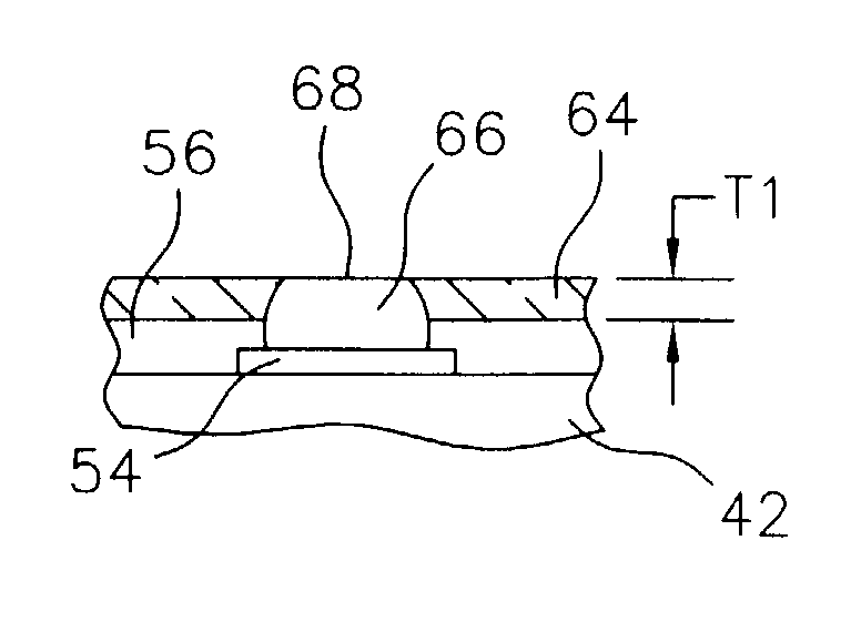
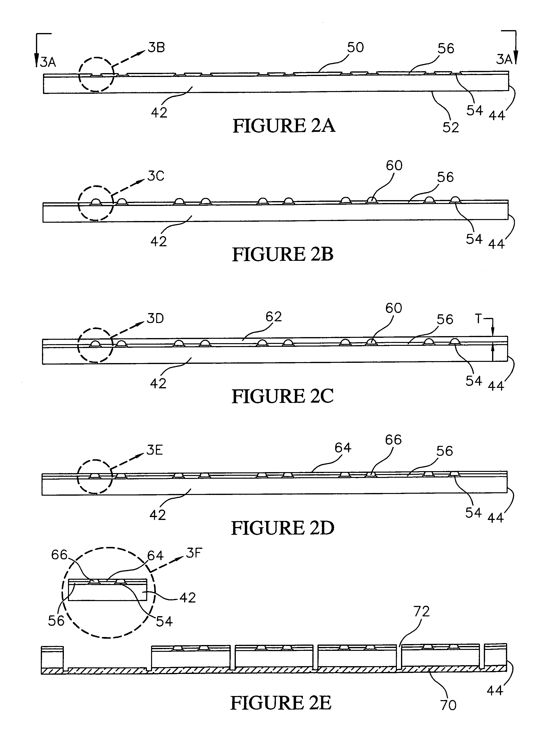
[0042]Referring to FIGS. 2A–2E, steps in the method for fabricating a board on chip (BOC) semiconductor package 40 (FIG. 4E) in accordance with the invention are illustrated.

[0043]Initially, as shown in FIGS. 2A and 3A, a plurality of semiconductor dice 42 are provided, for fabricating a plurality of BOC semiconductor packages 40 (FIG. 4E). The dice 42 can comprise conventional semiconductor dice having a desired configuration. For example, each die 42 can comprise a dynamic random access memory (DRAM), a static random access memory (SRAM), a flash memory, a microprocessor, a digital signal processor (DSP) or an application specific integrated circuit (ASIC). The dice 42 and the BOC packages 40 ...


PUM


Abstract

A semiconductor package includes a substrate, a die attached and wire bonded to the substrate, and a die encapsulant encapsulating the die. The die includes a circuit side having a pattern of die contacts, planarized wire bonding contacts bonded to the die contacts, and a planarized polymer layer on the circuit side configured as stress defect barrier. A method for fabricating the package includes the steps of forming bumps on the die, encapsulating the bumps in a polymer layer, and then planarizing the polymer layer and the bumps to form the planarized wire bonding contacts. The method also includes the steps of attaching and wire bonding the die to the substrate, and then forming the die encapsulant on the die.

Description

CROSS REFERENCE TO RELATED APPLICATIONS[0001]This application is a division of Ser. No. 10 / 192,736 filed on Jul. 10, 2002, U.S. Pat. No. 6,791,168 B1.FIELD OF THE INVENTION[0002]This invention relates generally to semiconductor packages and to methods of semiconductor packaging. More particularly, this invention relates to a semiconductor package having a die and a circuit side polymer layer on the die configured as a defect barrier. This invention also relates to a method for fabricating the package, and to systems incorporating the package.BACKGROUND OF THE INVENTION[0003]Different types of semiconductor packages have been developed recently with a smaller outline, and a higher pin count than conventional plastic or ceramic packages. These semiconductor packages are broadly referred to as BGA packages, chip scale packages or flip chip packages. One particular type of package is referred to as a board-on-chip (BOC) package.[0004]Referring to FIG. 1A, a prior art BOC package 10 is i...

Claims


Application Information

Patent Timeline
Patent Type & Authority Patents(United States)
IPC IPC(8): H01L23/495H01L21/56H01L21/60H01L23/31H01L25/065
CPCH01L24/27H01L24/29H01L24/32H01L21/561H01L21/565H01L21/6835H01L21/6836H01L23/13H01L23/3114H01L23/3128H01L23/3157H01L23/4951H01L23/49816H01L23/49827H01L24/03H01L24/05H01L24/06H01L24/11H01L24/12H01L24/16H01L24/48H01L24/49H01L24/83H01L24/94H01L24/97H01L25/0657H01L25/105H01L25/50H01L2224/48655H01L2224/48664H01L2224/48666H01L2224/48669H01L2224/48839H01L2224/48844H01L2224/48847H01L2224/48855H01L2224/48864H01L2224/48866H01L2224/48639H01L2224/48724H01L2224/48739H01L2224/48747H01L2224/48755H01L2224/48764H01L2224/48766H01L2224/48769H01L2924/00013H01L2225/1023H01L2225/107H01L2224/29299H01L2224/2929H01L2224/11334H01L2224/06135H01L2224/45155H01L2224/45164H01L2224/45169H01L2224/48091H01L2224/4824H01L2224/48247H01L2224/4826H01L2224/48465H01L2224/48471H01L2224/48472H01L2224/48479H01L2224/4943H01L2224/73215H01L2224/83101H01L2224/8319H01L2224/8385H01L2224/85444H01L2224/92H01L2224/92147H01L2224/92247H01L2224/97H01L2225/0651H01L2225/06555H01L2225/06558H01L2225/06568H01L2924/01005H01L2924/01006H01L2924/01013H01L2924/01022H01L2924/01027H01L2924/01028H01L2924/01029H01L2924/0103H01L2924/01042H01L2924/01046H01L2924/01047H01L2924/0105H01L2924/01073H01L2924/01074H01L2924/01077H01L2924/01078H01L2924/01079H01L2924/01082H01L2924/01083H01L2924/014H01L2924/07802H01L2924/14H01L2924/1433H01L2924/15153H01L2924/15165H01L2924/15311H01L2224/32245H01L24/45H01L2924/01023H01L2924/01033H01L2924/01087H01L2924/0665H01L2224/29101H01L2224/48624H01L2224/48644H01L2224/48647H01L24/85H01L2221/68327H01L2221/68377H01L2224/0401H01L2224/04042H01L2224/05001H01L2224/05073H01L2224/05111H01L2224/05118H01L2224/05155H01L2224/05556H01L2224/05624H01L2224/05639H01L2224/05644H01L2224/05647H01L2224/05655H01L2224/05664H01L2224/05666H01L2224/05669H01L2224/06136H01L2224/1132H01L2224/1134H01L2224/1147H01L2224/13099H01L2224/13139H01L2224/13144H01L2224/13147H01L2224/274H01L2224/2919H01L2224/32014H01L2224/32145H01L2224/32225H01L2224/451H01L2224/45111H01L2224/45118H01L2224/45124H01L2224/45139H01L2224/45144H01L2224/45147H01L2224/83H01L2224/85H01L2924/00014H01L2924/07025H01L2924/0635H01L2924/00H01L2224/48227H01L2924/00012H01L2924/3512H01L2224/48824H01L2224/48869H01L2224/48744H01L2224/29099H01L2224/29199H01L2224/45015H01L2924/181H01L2924/12042H01L2224/05554H01L2924/10161H01L2224/023H01L2924/20754H01L2224/45099H01L2224/4554H01L2924/0001
Inventor CONNELL, MIKEJIANG, TONGBI
Owner MICRON TECH INC
Why Eureka
Try Eureka