Silicon on insulator device having trench isolation layer and method for manufacturing the same

a technology of silicon on insulator and trench isolation layer, which is applied in the direction of semiconductor devices, semiconductor/solid-state device details, electrical apparatus, etc., can solve the problems of increasing junction capacitance, unstable operation characteristics of soi devices, and increasing leakage current, so as to prevent the gate insulating layer from deteriorating, stable operation characteristics, and low junction capacitance

Inactive Publication Date: 2006-02-07
SAMSUNG ELECTRONICS CO LTD
View PDF8 Cites 4 Cited by
  • Summary
  • Abstract
  • Description
  • Claims
  • Application Information

AI Technical Summary

Benefits of technology

[0032]According to the present invention, it is possible to provide a SOI device having low junction capacitance and stable operational characteristics. It is further possible to prevent the gate insulating layer from deteriorating and to manufacture a SOI device having high reliability by preventing a groove from being generated between a semiconductor layer and an isolation layer. In addition, it is possible to manufacture a SOI device by forming the isolation layer while preventing bending of the semiconductor layer. Finally, it is possible to prevent any increase in leakage current due to the dislocation defect.

Problems solved by technology

If the semiconductor layer 20 is bent, a defect, such as dislocation, may occur, and thus leakage current may be caused to increase.
The loaded electric charges cause a parasitic bipolar-induced breakdown or latch-up phenomenon and make the operational characteristics of the SOI device unstable.
The operational characteristics of the SOI device having the shallow isolation layer are stable; however, the SOI device having the shallow isolation layer has a problem in that junction capacitance increases because a junction portion is generated between the semiconductor layer and the source / drain region.
In addition, the gate insulating layer of the SOI device may deteriorate.
There is another problem with the conventional SOI device including an isolation layer having a dual trench structure.

Method used


Image

  • Silicon on insulator device having trench isolation layer and method for manufacturing the same
  • Silicon on insulator device having trench isolation layer and method for manufacturing the same
  • Silicon on insulator device having trench isolation layer and method for manufacturing the same

Examples


Embodiment Construction

[0039]The present invention will now be described more fully with reference to the accompanying drawings, in which a preferred embodiment of the invention is shown. This invention may, however, be embodied in many different forms and should not be construed as being limited to the embodiment set forth herein. Rather, this embodiment is provided so that this disclosure will be thorough and complete, and will fully convey the concept of the invention to those skilled in the art. In the drawings, the thickness of layers and regions are exaggerated for clarity. It will also be understood that when a layer is referred to as being “on” another layer or substrate, it can be directly on the other layer or substrate, or intervening layers may also be present.

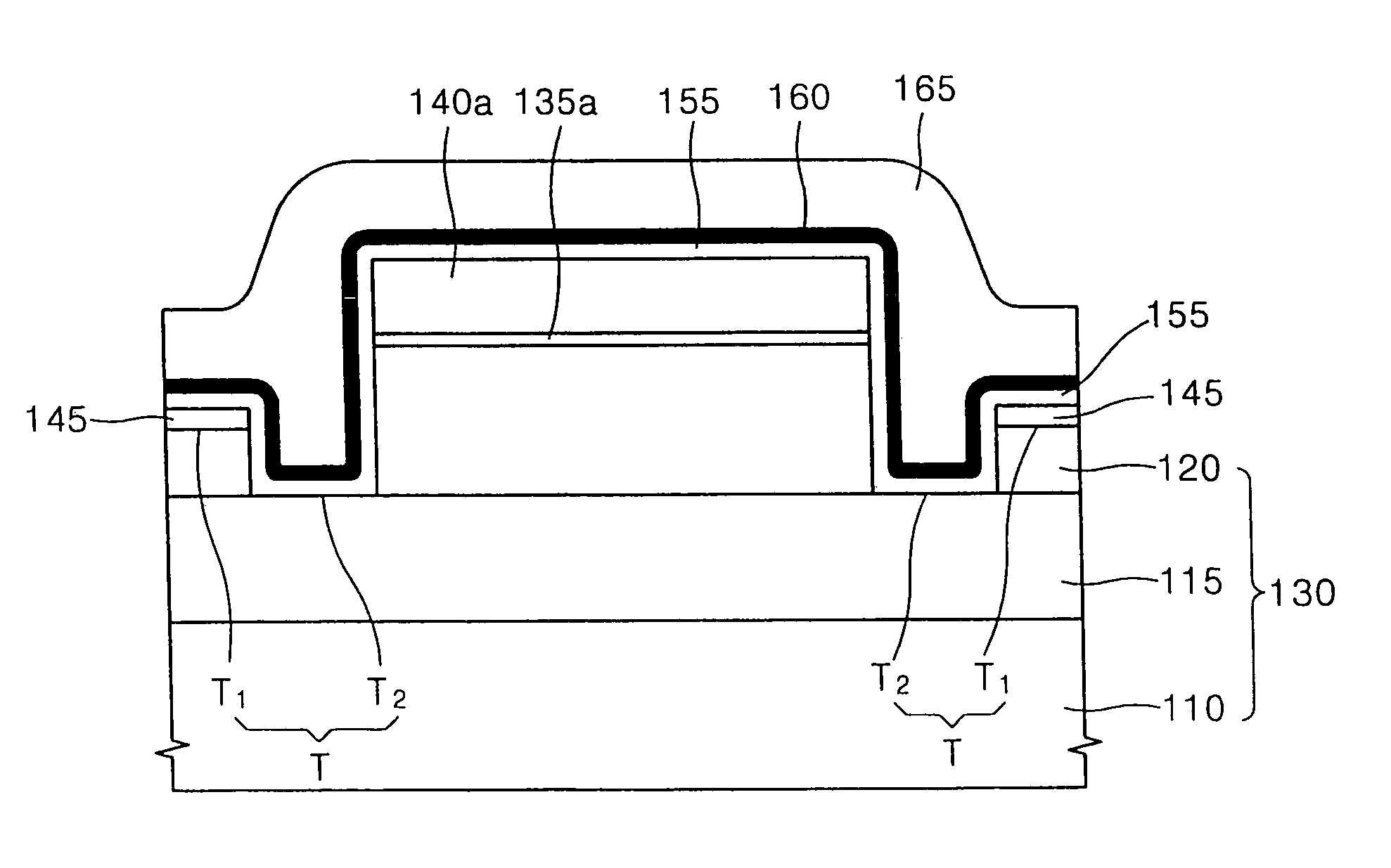
[0040]FIGS. 3 and 4A through 13B are views illustrating a semiconductor device and a method for manufacturing the same according to an embodiment of the present invention. Specifically, FIG. 3 is a schematic layout illustrating a semicon...


PUM


Abstract

A silicon-on-insulator (SOI) device and a method for manufacturing the same includes a substrate, which includes a base layer, a buried oxide layer, and a semiconductor layer, and an isolation layer which is formed in a trench that defines an active region on the semiconductor layer. The trench comprises a first region having a depth smaller than the thickness of the semiconductor layer and a second region having a depth as much as the thickness of the semiconductor layer. The isolation layer includes an oxide layer and a nitride liner that are sequentially formed along the surface of the trench and a dielectric layer that fills the trench.

Description

RELATED APPLICATION[0001]This application is a divisional of U.S. application Ser. No. 10 / 114,215, filed on Apr. 2, 2002, now U.S. Pat. No. 6,737,706 which relies for priority upon Korean Patent Application No. 01-45693, filed on Jul. 28, 2001, the contents of which are herein incorporated by reference in their entirety.BACKGROUND OF THE INVENTION[0002]1. Field of the Invention[0003]The present invention relates to a semiconductor device and a method for manufacturing the same, and more particularly, to a semiconductor device using a silicon-on-insulator (SOI) substrate (hereinafter, referred to as a “SOI device”) and method for manufacturing the same.[0004]2. Description of the Related Art[0005]A SOI substrate, unlike a bulk silicon substrate, has a stacked structure including a base layer, providing a supporting means, a buried oxide layer, and a semiconductor layer, on which devices are formed. SOI devices integrated on such a SOI substrate can be completely isolated from one ano...

Claims


Application Information

Patent Timeline
Patent Type & Authority Patents(United States)
IPC IPC(8): H01L29/00H01L27/01H01L29/40H01L29/76H01L21/76H01L21/336H01L27/00H01L21/762H01L27/12H01L29/786
CPCH01L21/76264H01L29/78636H01L29/78615H01L29/66772H01L21/76283H01L21/76
Inventor LEE, TAE-JUNGKIM, BYUNG-SUNOH, MYOUNG-HWANYOO, SEUNG-HANSHIN, MYUNG-SUNPARK, SANG-WOOK
Owner SAMSUNG ELECTRONICS CO LTD
Why Eureka
Try Eureka