BIST circuit for measuring path delay in an IC

a path delay and circuit technology, applied in the field of built-in/self-testing (bist) circuits, can solve the problems of ic manufacturers finding it more difficult and time-consuming to use a general-purpose ic tester, ic cannot function properly, and the “path delay” that it measures is neither

Inactive Publication Date: 2006-02-07
CREDENCE SYSTEMS
View PDF8 Cites 37 Cited by
  • Summary
  • Abstract
  • Description
  • Claims
  • Application Information

AI Technical Summary

Problems solved by technology

But as integrated circuits (ICs) have become larger and more complex, IC manufacturers have found it more difficult and time-consuming to use a general purpose IC tester to test every sub-circuit of a large IC.
For example, large ICs often include “embedded circuits” such memories that other circuits within an IC access but which are not directly accessible through an IC's I / O terminals and which an external tester therefore cannot directly access.
An IC can fail to function properly when a delay through a signal path within the IC is too long or too short.
A signal path will typically delay rising and falling edges of a signal by differing amounts due to the lack of symmetry in the switching speeds of logic gates forming the signal path.
One drawback to the BIST circuit described by Sunter et al is that the “path delay” that it measures is neither the rising edge delay nor the falling edge delay but the average of the two.
While this system can separately measure rising and falling edge path delays, one difficulty with this system is that during the calibration process, the delay through the programmable delay circuit cannot really be set to zero since all programmable delay circuits have some residual delay when they are at their lowest setting.
Thus, the delay provided by the calibration process exceeds the expected delay at least by the amount of the residual delay which can be a considerable amount compared to the path delay to be measured.
Another drawback is that the system does not account for differences in path delays the first and second strobe signals may experience as they travel to the latch, so it is important when laying out an IC to make sure that the two paths closely match one another.
The calibration circuit taught by Gillis is also relatively complicated, including an arithmetic logic unit, several counters and registers and the like along with sequencing logic capable of controlling operations of all of these parts.

Method used


Image

  • BIST circuit for measuring path delay in an IC
  • BIST circuit for measuring path delay in an IC
  • BIST circuit for measuring path delay in an IC

Examples


Embodiment Construction

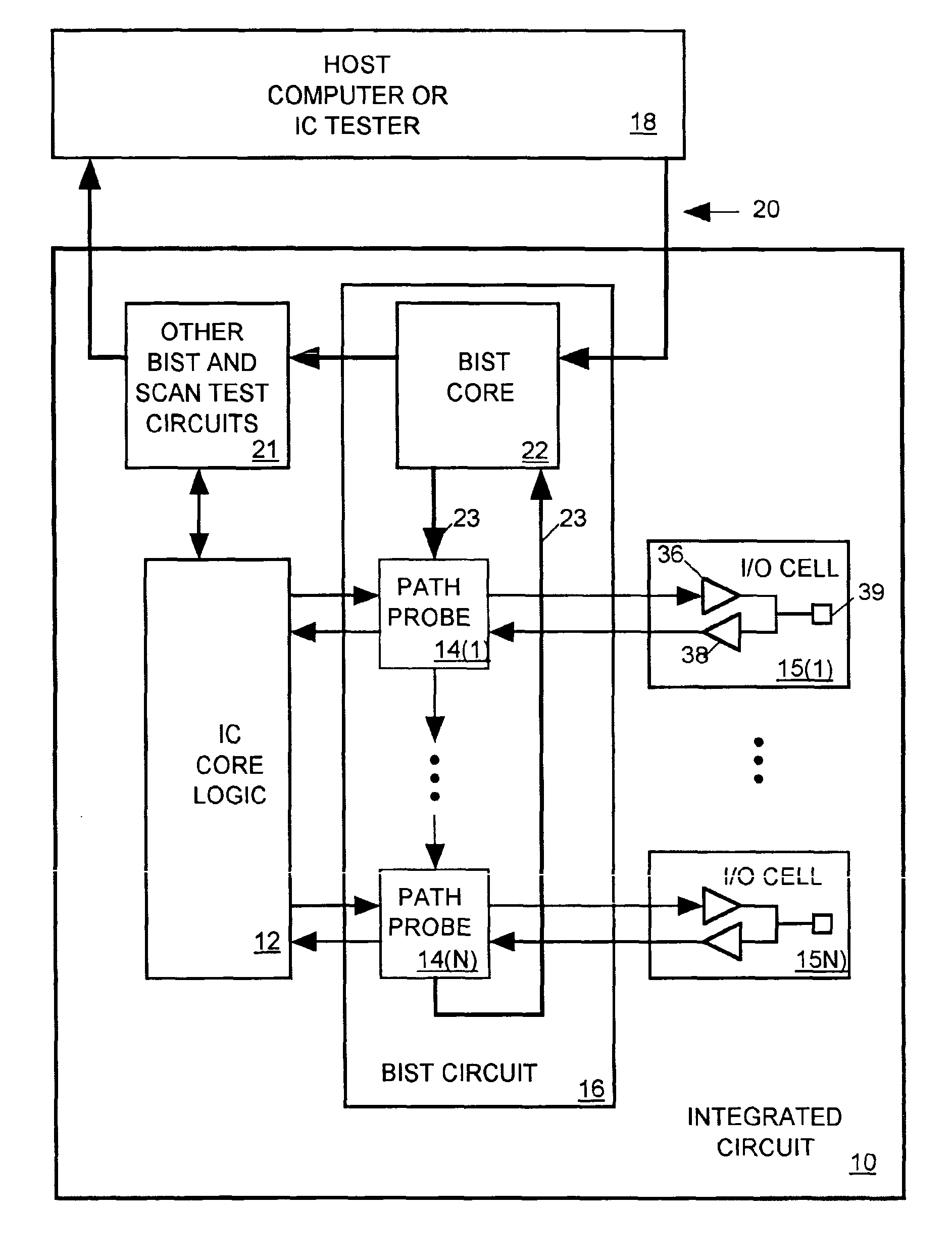
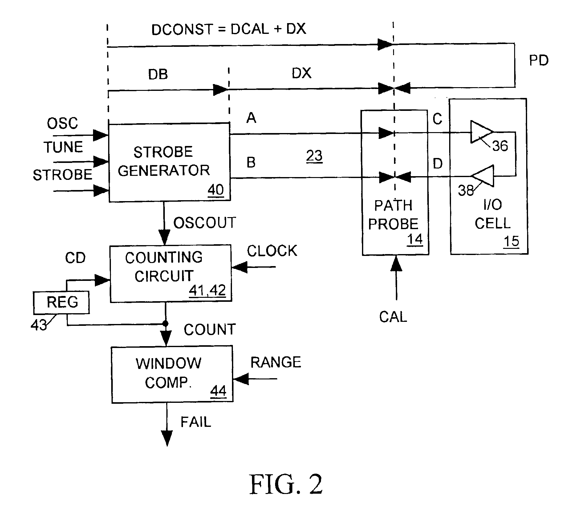
[0026]The invention relates to a built-in / self-test (BIST) circuit that may be included within an integrated circuit (IC) for determining whether a rising or falling edge delay through a signal path within the IC is within acceptable limits. For illustrative purposes, the BIST circuit is described below as being used to measure a path delay through an input / output (I / O) cell of an IC, but a BIST circuit in accordance with the invention can be used to measure a path delay through any signal path within an IC that produces a rising or falling output signal edge in delayed response to a rising or falling input signal edge.

IC Architecture

[0027]FIG. 1 illustrates in block diagram form an IC 10 including core logic 12 for carrying out the logic performed by the IC. Core logic 12 communicates with circuits outside IC 10 through a set of I / O cells 15(1)-15(N), each including a driver 36 and a receiver 38 connected to a pad 39 providing a point of connection for external circuits. IC 10 incl...


PUM

PropertyMeasurementUnit
currentaaaaaaaaaa
capacitanceaaaaaaaaaa
switching speedsaaaaaaaaaa

Abstract

A BIST circuit for an IC measures the time delay a rising or falling edge experiences as it passes through a signal path within the IC. A strobe circuit within the BIST circuit generates edges in two signals A and B in delayed response to edges of a STROBE signal. A path probe generates a signal C edge at the signal path input in response to each signal A edge. The STROBE-to-B edge delay within the strobe generator is iteratively adjusted to determine a first delay for which the path probe detects the B and C signal edges at nearly the same time and thereafter iteratively adjusted to determine a second delay for which the path probe detects the B and D signal edges at nearly the same time. The first delay is measured by causing the strobe signal generator to produce a periodic signal having a period proportional to the first delay and counting the number of cycles of a reference clock occurring during K cycles of the periodic signal. The second delay is measured in a similar manner. The path delay is determined as a difference between the measured first and second delays.

Description

CROSS-REFERENCE TO RELATED APPLICATIONS[0001]The present application discloses subject matter in common with a copending U.S. patent application entitled “SELF-CALIBRATING STROBE SIGNAL GENERATOR” Ser. No.10 / 628,995 filed concurrently herewith.BACKGROUND OF THE INVENTION[0002]1. Field of the Invention[0003]The present invention relates in general to built-in / self-test (BIST) circuits and in particular to a BIST circuit for determining whether a path delay within and integrated circuit (IC) is within acceptable limits.[0004]2. Description of Related Art[0005]Integrated circuit (IC) manufacturers often use general purpose IC testers to test ICs by applying test signals to their I / O terminals and monitoring the IC's output signals to see how they respond to the test signal. But as integrated circuits (ICs) have become larger and more complex, IC manufacturers have found it more difficult and time-consuming to use a general purpose IC tester to test every sub-circuit of a large IC. For ...

Claims


Application Information

Patent Timeline
Patent Type & Authority Patents(United States)
IPC IPC(8): G04F10/00G01R31/28G01R31/00G01R31/30G01R31/317G06K5/04G11B5/00G11B20/20
CPCG01R31/31725G01R31/3016
Inventor GANRY, OLIVIER
Owner CREDENCE SYSTEMS
Why Eureka
Try Eureka