Method for producing a surface acoustic wave element

a surface acoustic wave and element technology, applied in piezoelectric/electrostrictive transducers, device material selection, transducer types, etc., can solve the problems of difficult to achieve a sharp cut-off property in the temperature range used, conventional difficult to handle surface acoustic wave elements, etc., to achieve reliable and inexpensive production, easy to handle, and low cost

Inactive Publication Date: 2006-02-14
SKYWORKS PANASONIC FILTER SOLUTIONS JAPAN
View PDF25 Cites 13 Cited by
  • Summary
  • Abstract
  • Description
  • Claims
  • Application Information

AI Technical Summary

Benefits of technology

[0008]It is an object of the present invention to provide a surface acoustic wave element that can be handled easily and has few defects and a surface acoustic wave device using the same. It is another object of the present invention to provide a method for producing a surface acoustic wave element that allows a surface acoustic wave element to be produced reliably and inexpensively by preventing the generation of defects in the process of separating into elements.

Problems solved by technology

In the case where a band in which signals are sent out is close to a band in which signals are received, as seen in the recent mobile communication systems, it is difficult to achieve a sharp cut-off property in the temperature range used.
However, the conventional surface acoustic wave element as described above has the following problems.
Since it has a laminate structure where the piezoelectric single crystal several tens of μm thick and the glass substrate are laminated, it is difficult to handle the surface acoustic wave element.
For example, in mounting the surface acoustic wave element on a package, in particular, in picking up the surface acoustic wave element, cracking or fracturing may occur in the piezoelectric single crystal layer.
Moreover, in dividing a wafer into individual surface acoustic wave elements, when it is cut with a cutting blade selected based on the glass substrate, fracturing or chipping may occur in the piezoelectric single crystal portion during cutting because of the difference in the characteristics between the materials.

Method used


Image

  • Method for producing a surface acoustic wave element
  • Method for producing a surface acoustic wave element
  • Method for producing a surface acoustic wave element

Examples


embodiment 1

[0042]In Embodiment 1, an example of a surface acoustic wave element of the present invention will be described.

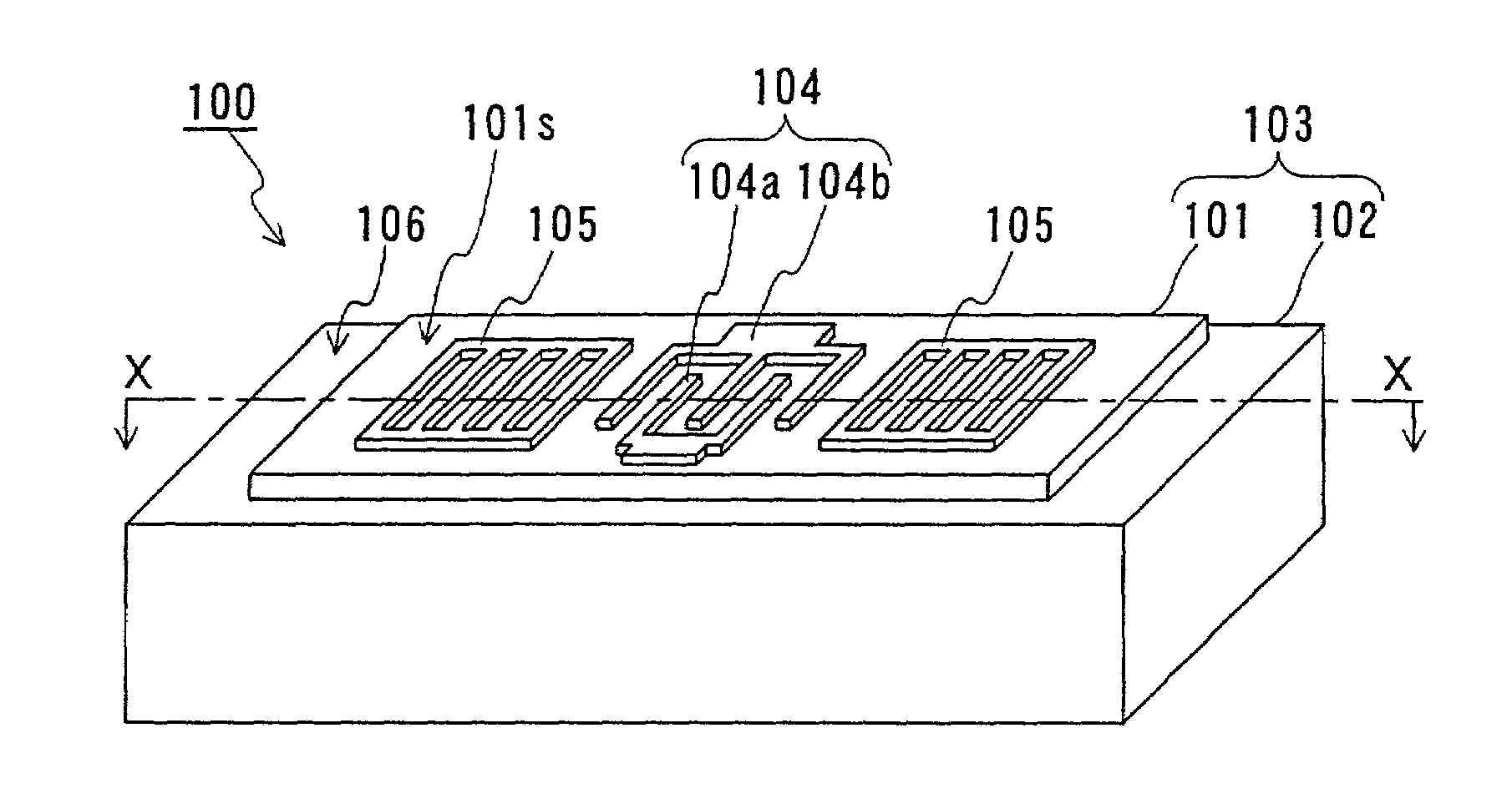
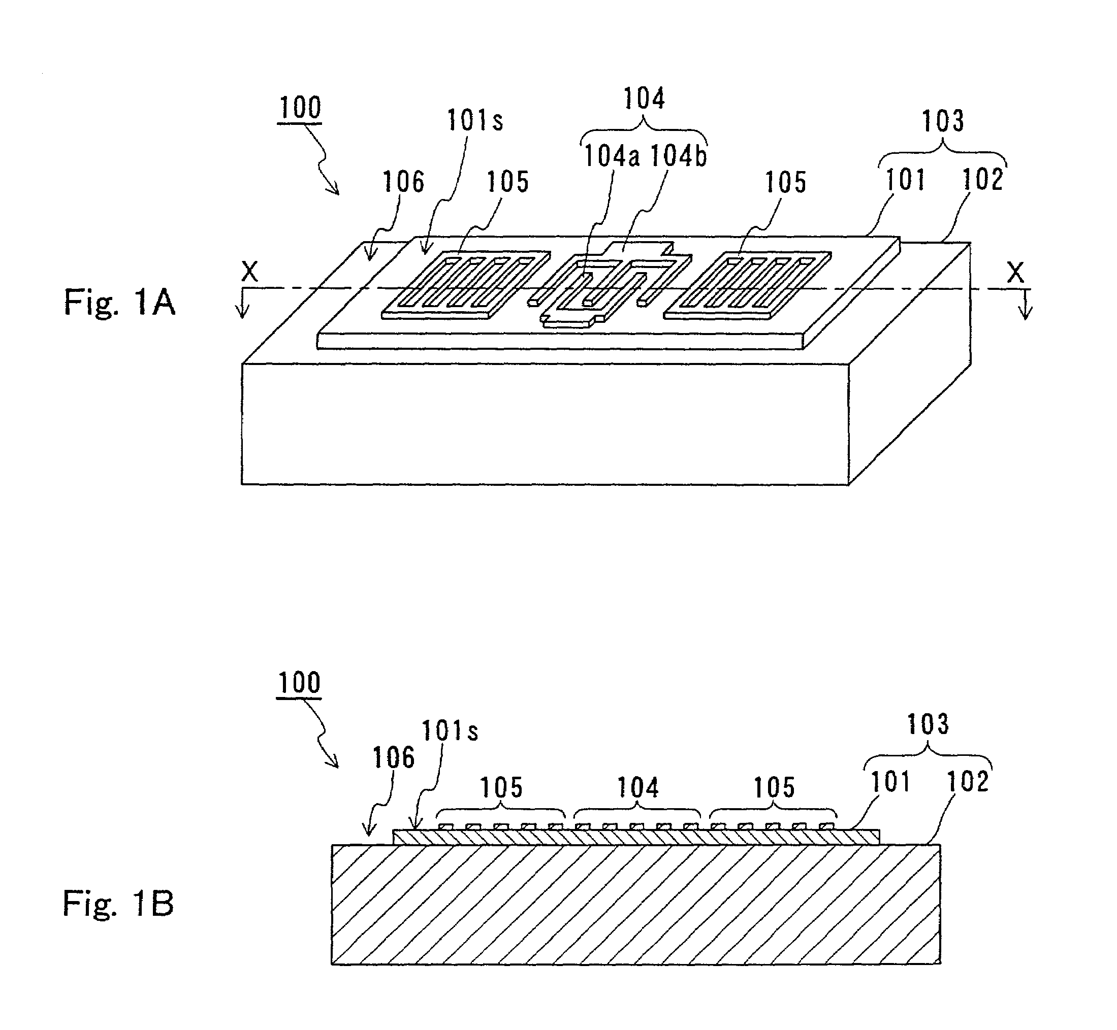
[0043]FIG. 1A is a perspective view of a surface acoustic wave element 100 of Embodiment 1, and FIG. 1B is a cross-sectional view thereof taken along line X—X in FIG. 1A.

[0044]Referring to FIGS. 1A and 1B, the surface acoustic wave element 100 includes a laminated substrate 103 comprising a first substrate 101 and a second substrate 102, a comb-shaped electrode 104, and a reflector 105. A step 106 is formed on the periphery (side face) of the laminated substrate 103 on the side of the first substrate 101.

[0045]The first substrate 101 is made of a piezoelectric material, and for example, a piezoelectric single crystal can be used. Examples of the piezoelectric single crystal include lithium tantalate, lithium niobate, quartz crystal, and Langasite. More specifically, a 36° Y-cut X-propagating lithium tantalate can be used, for example. The thickness of the first substrate 1...

embodiment 2

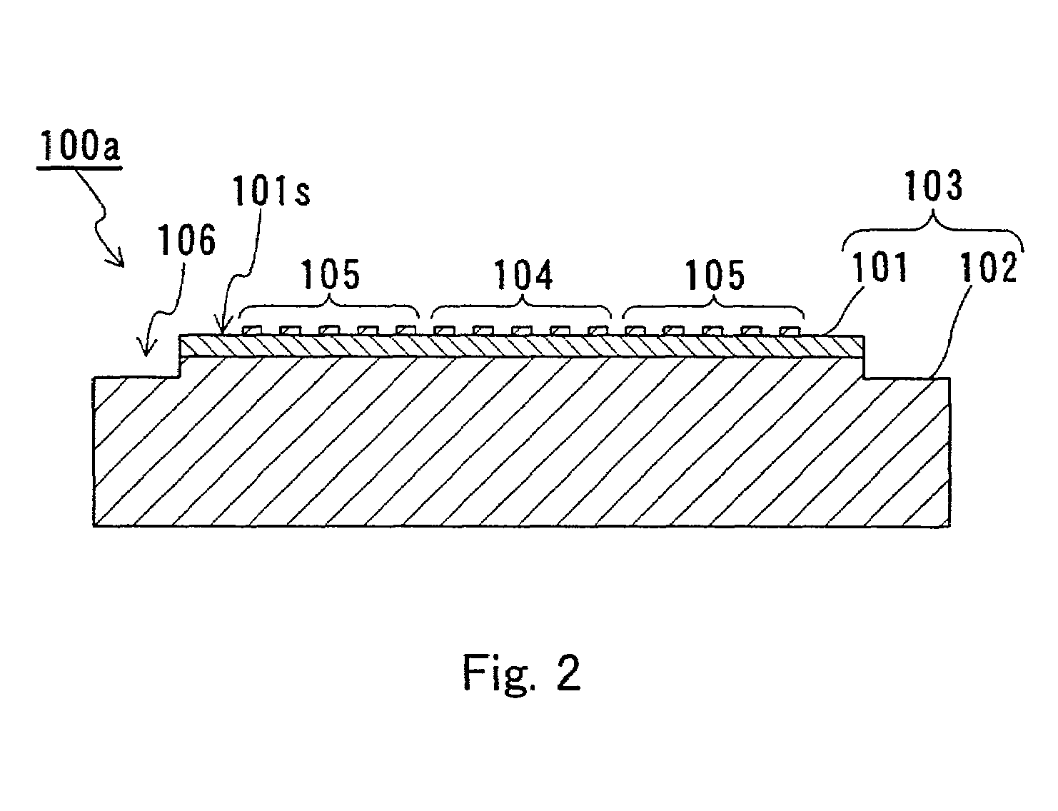
[0054]In Embodiment 2, another example of the surface acoustic wave element of the present invention will be described. The description of the same parts as those described in Embodiment 1 will be omitted.

[0055]FIG. 6A is a perspective view of a surface acoustic wave element 200 of Embodiment 2, and FIG. 6B is a cross-sectional view thereof taken along line Y—Y in FIG. 6A.

[0056]Referring to FIGS. 6A and 6B, the surface acoustic wave element 200 includes a laminated substrate 103 comprising a first substrate 101 and a second substrate 102, a comb-shaped electrode 104 formed on a surface 101s of the first substrate 101, and a reflector 105. A notch 201 is formed on the periphery of the laminated substrate 103 on the side of the first substrate 101.

[0057]The notch 201 is formed on the side face of the laminated substrate 103 where the comb-shaped electrode 104 is formed. In other words, the notch 201 is formed on the periphery of the laminated substrate 103 on the side of the first sub...

embodiment 3

[0062]In Embodiment 3, an example of a method for producing the surface acoustic wave element 100 described in Embodiment 1 will be described. The description of the same parts as those described in Embodiment 1 will be omitted.

[0063]Referring to FIGS. 9A to 9E, in the method of Embodiment 3, first, as shown in FIG. 9A, a first substrate 101a (having a thickness of, for example 0.2 mm), which will be the first substrate 101, is laminated directly on joined to) a second substrate 102a (having a thickness of, for example 1 mm), which will be the second substrate 102. In this embodiment, the first substrate 101a having a thickness of 0.2 mm and the second substrate 102a having a thickness of 1 mm are used as the starting materials and joined together. However, this is only an example, and the materials can be selected in view of handling in a substrate cleaning process, ensuring parallelism and smoothness of each substrate, or the like. There are no particular limitations regarding the...


PUM

PropertyMeasurementUnit
thickaaaaaaaaaa
thickaaaaaaaaaa
thicknessaaaaaaaaaa

Abstract

A surface acoustic wave element includes a laminated substrate where a first substrate made of a piezoelectric material is laminated over a second substrate made of a material different from that of the first substrate, and at least one pair of comb-shaped electrodes formed on one main plane of the first substrate. A step or a notch is formed on the periphery of the laminated substrate on the side of the first substrate.

Description

[0001]This application is a divisional of application Ser. No. 09 / 587,938, now U.S. Pat. No. 6,426,583 filed Jun. 6, 2000, which application(s) are incorporated herein by reference.BACKGROUND OF THE INVENTION[0002]1. Field of the Invention[0003]The present invention relates to a surface acoustic wave element including a laminated substrate, a method for producing the same and a surface acoustic wave device using the same.[0004]2. Description of the Related Art[0005]In the development of mobile communication equipment, it is desired to achieve high performance of a surface acoustic wave element, which is one of the key devices constituting the equipment. In the case where a band in which signals are sent out is close to a band in which signals are received, as seen in the recent mobile communication systems, it is difficult to achieve a sharp cut-off property in the temperature range used. This is due to the characteristics of a piezoelectric substrate used in conventional surface ac...

Claims


Application Information

Patent Timeline
Patent Type & Authority Patents(United States)
IPC IPC(8): H04R17/00H01L41/09H01L41/18H01L41/22H01L41/312H01L41/337H03H9/02H03H9/10H03H9/145
CPCH03H9/0222H03H9/02566H03H9/02574H03H9/02629H03H9/02669H03H9/02834H03H9/1071H03H9/1085H03H9/02984Y10T29/49126Y10T29/49135Y10T29/42Y10T29/49005Y10T29/49128
Inventor ONISHI, KEIJISATO, HIROKITOMITA, YOSHIHIRO
Owner SKYWORKS PANASONIC FILTER SOLUTIONS JAPAN
Why Eureka
Try Eureka