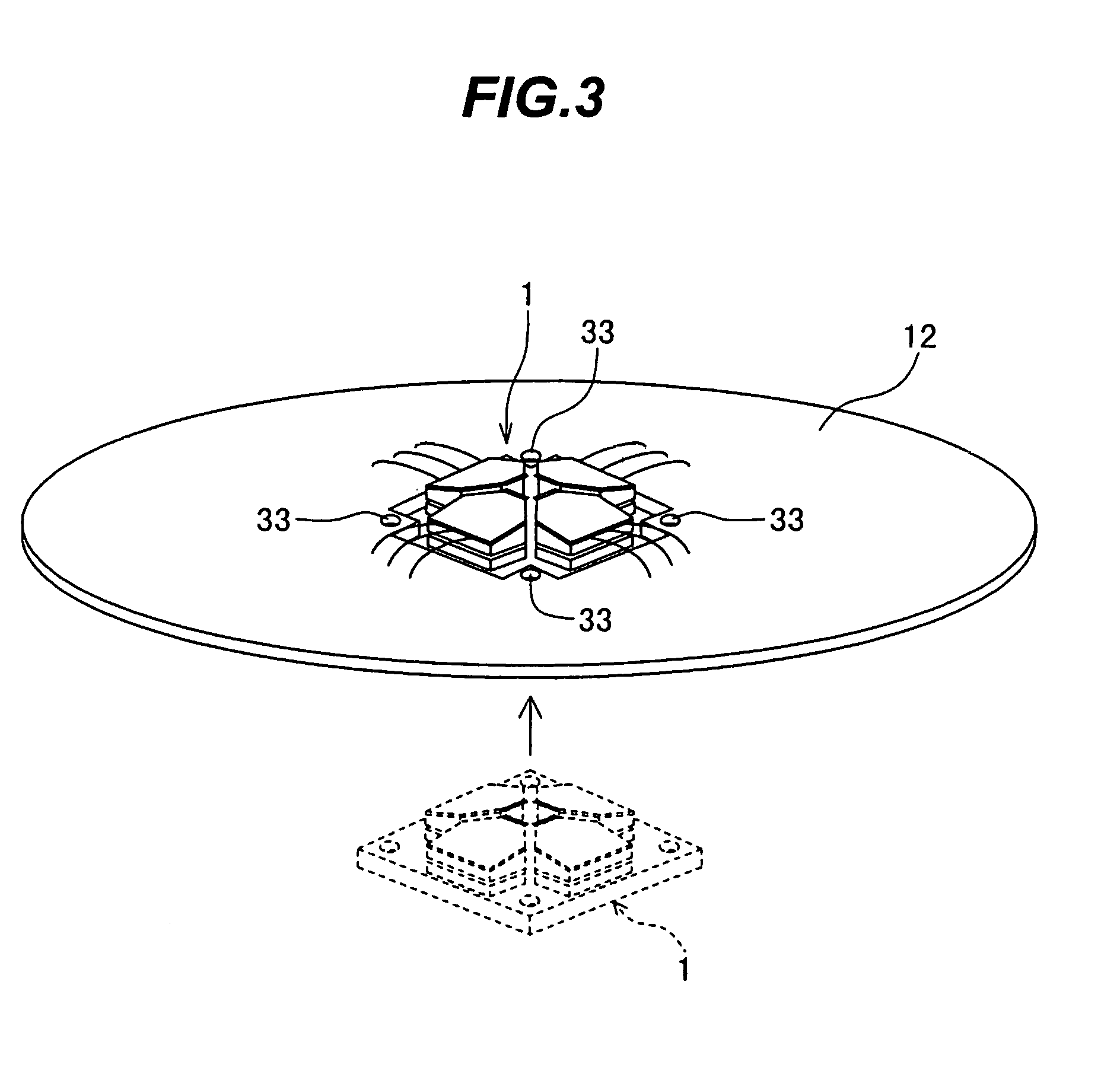
[0011]In order to achieve the above-described object, the present invention provides a probe head comprising: a table having a flat slide plane; a plurality of slide units each having a slide surface for sliding on the flat slide plane; a lift unit provided for each of the slide units, the lift unit being capable of moving along a vertical direction; probes provided for each of the lift units, a top end of each of the probes protruding from the lift unit; and positioning means for positioning the lift unit relative to the slide unit and the slide unit relative to the table. By sliding the slide unit on the flat slide plane, the relative positions of the plurality of slide units can be adjusted along the direction parallel to the flat slide plane. Even if the slide unit together with the lift unit moves along the direction parallel to the flat slide plane, the relative positions of the plurality of lift units will not change along the direction vertical to the flat slide plane. Namely, by sliding the slide units on the flat slide plane of the table and moving the lift units along the direction vertical to the flat slide plane, the relative positions of the plurality of probes provided for each lift unit can be adjusted separately and independently for each of the directions parallel to and vertical to the flat slide plane. According to the invention, therefore, since the relative positions of the probes can be adjusted separately and independently for each of the z- y- and z-directions which are mutually perpendicular, the relative positions of the probes can be adjusted at a high precision.
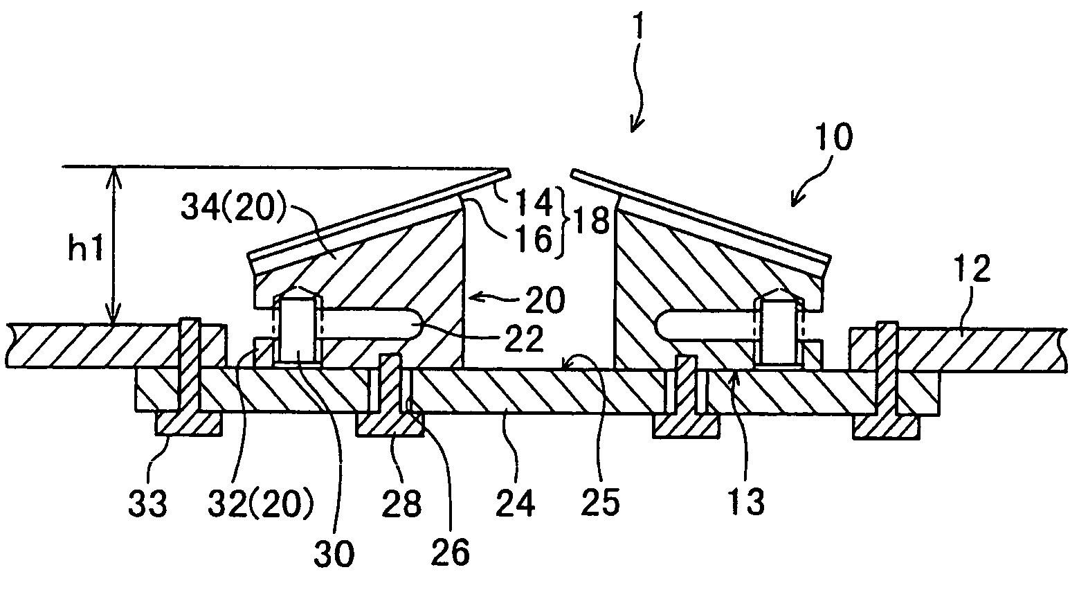
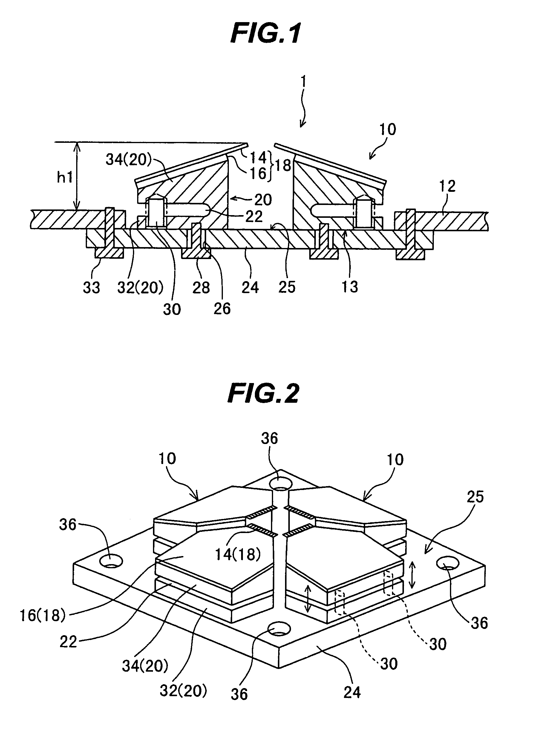
[0013]In the probe head of this invention, the lift unit comprises a movable unit integrally formed with the slide unit and having one end connected to the slide unit and another end made as a free end, and a support unit fixed to the movable unit and disposed with the probes, and the positioning means includes a screw threaded into the slide unit for moving the movable unit along a direction extending remote from the slide surface and along a direction extending near to the slide surface. The movable unit integrally formed with the slide unit is made movable in a direction vertical to the slide surface, so that the number of components can be reduced. Specifically, the movable unit having one end connected to the slide unit and the other end made as a free end is formed integrally with the slide unit and the position of the movable unit is determined by screws, so that the number of components can be reduced.
[0015]In the probe head of this invention, the slide unit includes guide means for guiding the lift unit slidably along a direction inclined relative to the slide surface. Since the lift unit can slide relative to the slide unit along the direction inclined relative to the slide surface, the number of components can be reduced.
[0016]In the probe head of this invention, the lift unit comprises a movable unit for sliding along the direction inclined relative to the slide surface by being guided by the guiding means, a support unit disposed with the probes and an engagement unit for detachably engaging the support unit with the movable unit. The movable unit capable of sliding along the direction inclined relative to the slide surface and the support unit disposed with the probes are made as discrete components mutually detachable. Therefore, when the probes along with the support unit are replaced, the positions and postures of the probes relative to the table are not required to be adjusted again to obtain the adjustment state before replacement. The probe head of this invention further comprises an elastic member interposed between the lift unit and the slide unit, wherein the positioning means includes a screw threaded into the lift unit and the slide unit. Deformation of the elastic member interposed between the lift unit and the slide unit allows the movable unit to move along the direction vertical to the slide surface. The position of the lift unit can therefore be determined without any play.
[0019]In order to achieve the above-described object, the invention provides a probe card comprising: a printed circuit board; a support unit whose position is determined relative to the printed circuit board; probes held by the support unit; adjusting means for adjusting a position or posture of the support unit relative to the printed circuit board; and wires electrically connecting the probes to electrodes of the printed circuit board. Since the wires can be bent easily, the wires interconnecting the probes and electrodes of the printed circuit board facilitate to adjust omnidirectionally and freely the positions and postures of the probes relative to the printed circuit board. According to the invention, therefore, the positions and postures of the probes can be adjusted at a high precision.
[0020]In order to achieve the above-described object, the invention provides a probe card comprising: a printed circuit board; a support unit whose position is determined relative to the printed circuit board; probes held by the support unit; adjusting means for adjusting a position or posture of the support unit relative to the printed circuit board; and a flexible printed circuit board having flying leads whose top ends are connected to the probes or electrodes of the printed circuit board, the flexible printed circuit board electrically connecting the probes and the electrodes of the printed circuit board. Since the wires can be bent easily, the wires interconnecting the probes and electrodes of the printed circuit board facilitate to adjust omnidirectionally and According to the invention, therefore, the positions and postures of the probes can be adjusted at a high precision. Furthermore, since the proximal ends of the plurality of flying leads are fixed to the printed circuit board, it is possible to improve the
work performance of a process of connecting the distal ends of the flying leads to the electrodes.

