

Liquid crystal display device and drive method thereof
a technology of liquid crystal display and drive method, which is applied in the direction of identification means, instruments, optics, etc., can solve the problems of serious deterioration in display quality, increase in drive voltage, and significant increase in the cost so as to reduce the overall power consumption of a driver ic for driving the video signal line, the effect of drastically reducing the possibility of cross-talk
- Summary
- Abstract
- Description
- Claims
- Application Information
AI Technical Summary
Benefits of technology
Problems solved by technology
Method used
Image

Examples
embodiment 1
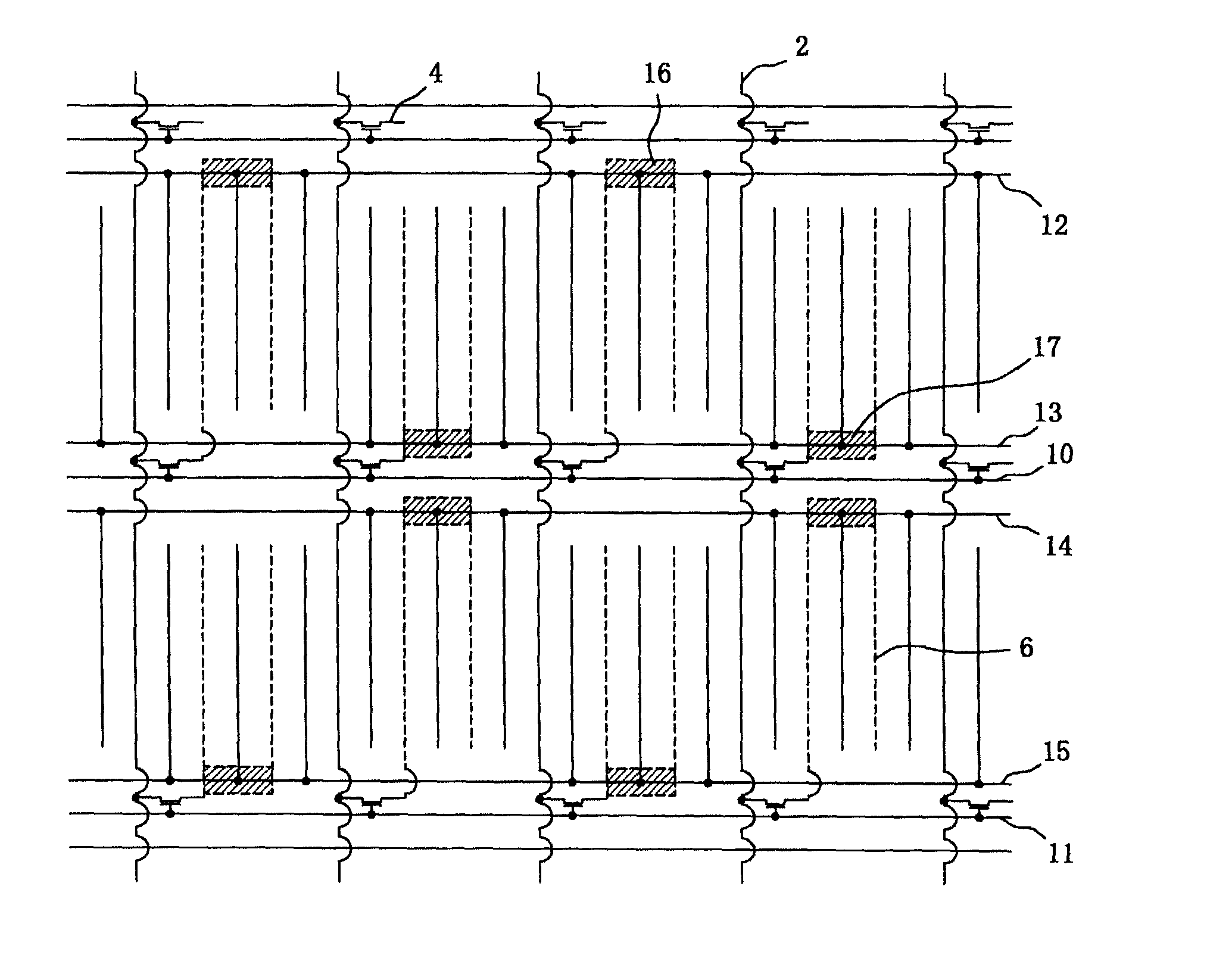
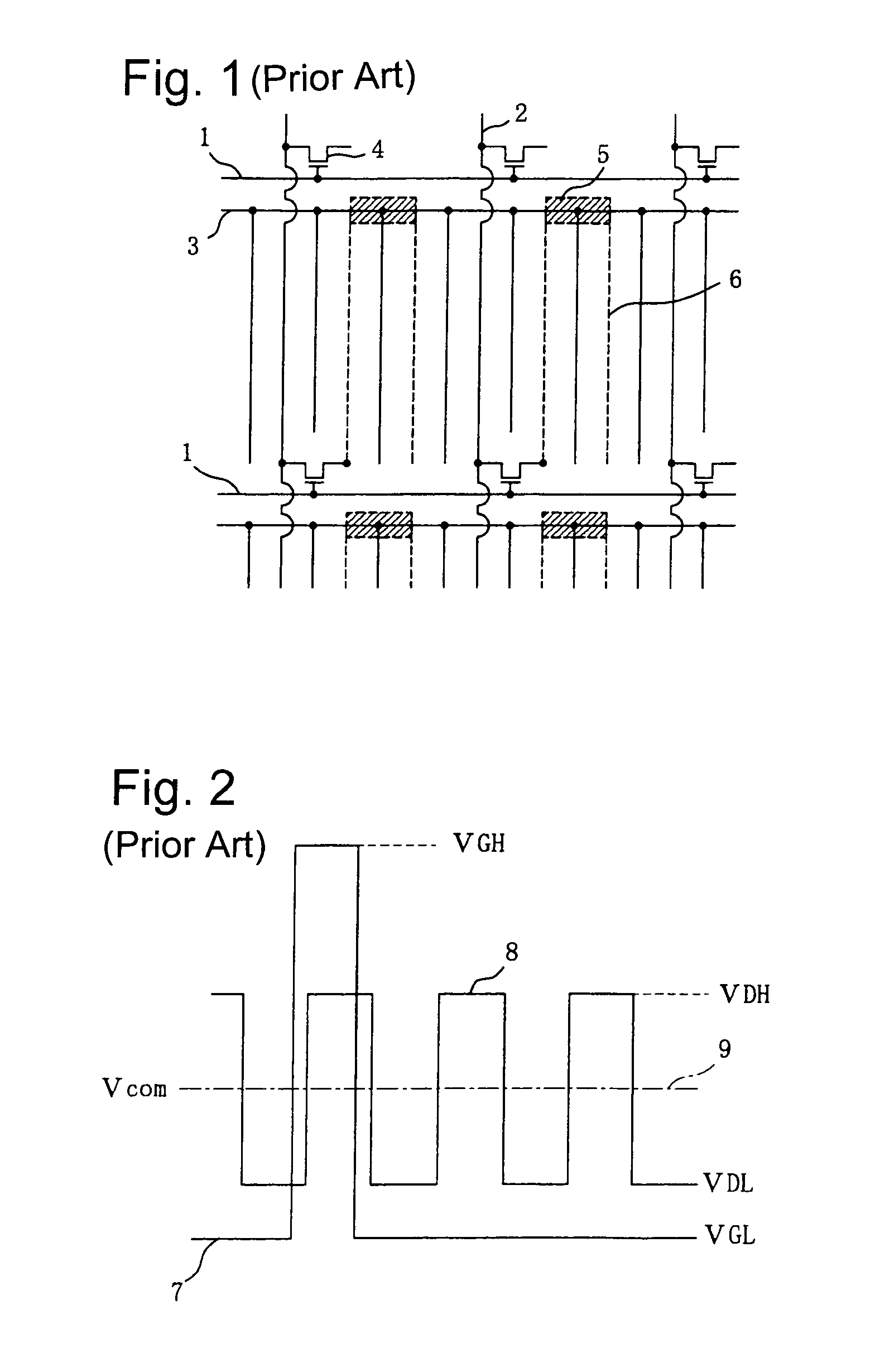
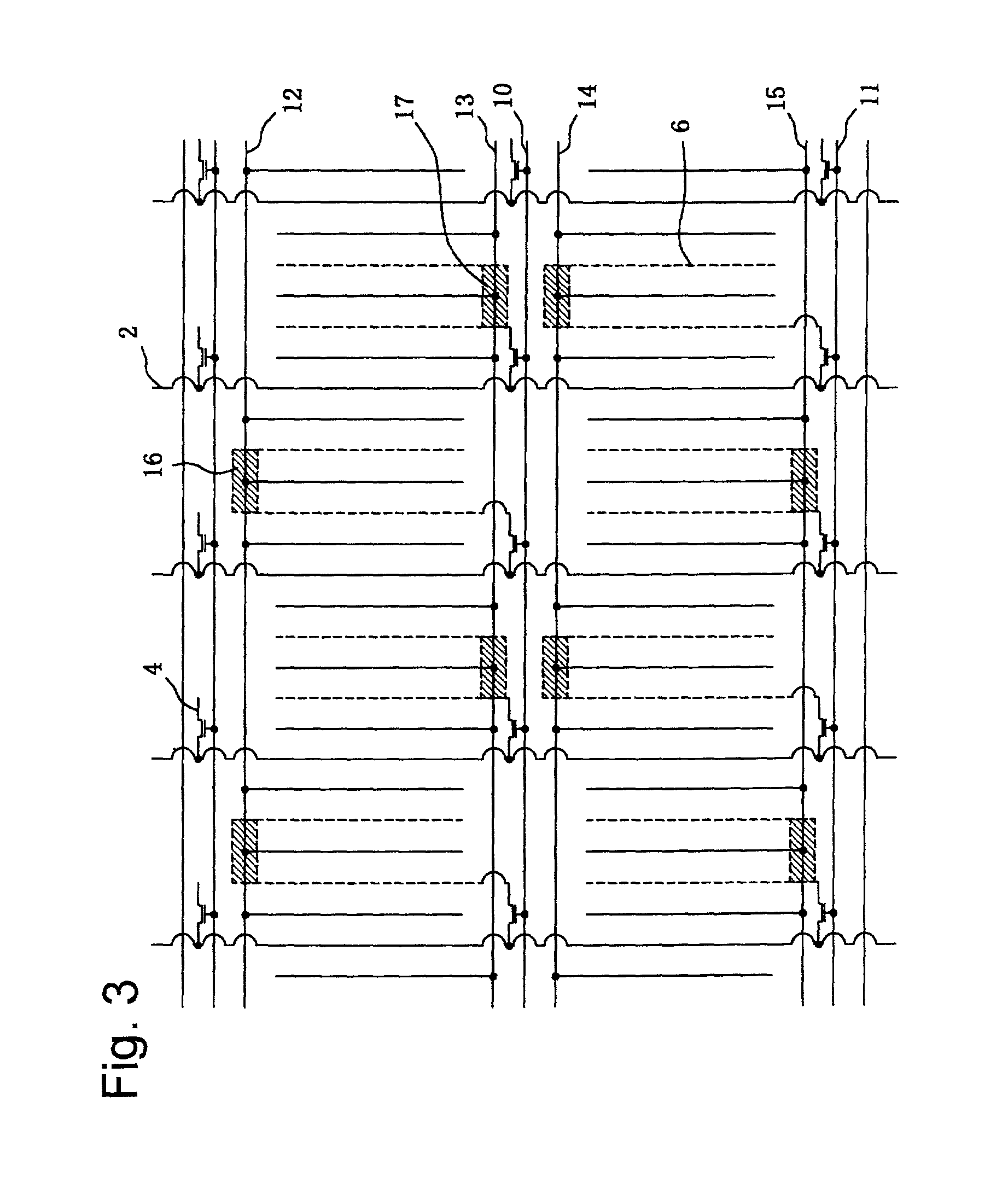
[0093]FIGS. 3 and 11 are plan views of the liquid crystal display panel in the first embodiment of the present invention. As shown in the drawings, an active matrix type liquid crystal display device of the present invention includes scanning lines 10 and 11 which are parallel to each other, and video signal lines 2 which are perpendicular to the scanning lines 10 and 11. The scanning lines 10 and 11 and video signal lines 2 are formed on a glass substrate (shown in FIG. 13). The scanning lines 10 and 11 and the video signal lines 2 are also arranged in a matrix format, where each grid denotes a unit pixel.
[0094]It should be noted that, within the context of this invention, such terms as “parallel”, “perpendicular”, “upward”, “vertical”, etc. should not be interpreted with strict and narrow meanings but be interpreted with wider meaning within the concept of this invention. For example, the word “parallel” should be interpreted as roughly or almost parallel in such a degree that two...
embodiment 2
[0121]FIGS. 4 and 5 are plan views of the liquid crystal display device in the second embodiment of the present invention. The arrangement of the common electrodes 12–15 within the unit pixel is the same as that in the first embodiment. In the first embodiment of the active matrix type liquid crystal display device described above, the hold capacitor is formed by the crossing of the liquid crystal drive electrode 6 (liquid crystal drive electrode 27) and one of the common electrodes 12–15. However, in the second embodiment, the formation of the hold capacitor is different from the first embodiment. Here, the parts similar to the first embodiment will be denoted by the same reference numbers, and their explanation of which will be omitted.
[0122]In FIG. 4, a hold capacitor 18 in the second embodiment is formed by the scanning line 10 and the liquid crystal drive electrode 6. Namely, the hold capacitor 18 is established by sandwiching the gate insulation layer 26 (such as shown in FIGS...
embodiment 3
[0125]FIGS. 6 and 14 are plan views of the liquid crystal display device in the third embodiment of the present invention. The arrangement of the common electrodes 12–15 in the unit pixel is the same as that of the first embodiment. In the third embodiment, the video signal line 2, the common electrodes 12–15, and the liquid crystal drive electrode 6 are bent relative to the alignment direction of the liquid crystal. With respect to the common electrodes 12–15, the part forming the comb-like electrodes are bent. Here, the components which are the same or similar to the first and second embodiments are denoted with the same reference numbers and the explanation of which is omitted.
[0126]In FIG. 6, the comb-like electrodes of the common electrodes 12–15, the video signal line 2, and the liquid crystal drive electrode 6 are diagonally aligned in a parallel fashion with one another. At the about the center of each pixel, the diagonally aligned such lines and electrodes are bent in an op...
PUM
| Property | Measurement | Unit |
|---|---|---|
| intersecting angle | aaaaa | aaaaa |
| intersecting angle | aaaaa | aaaaa |
| intersecting angle | aaaaa | aaaaa |
Abstract
Description
Claims
Application Information