Method of fabricating liquid crystal display

a liquid crystal display and liquid crystal technology, applied in the field of liquid crystal display, can solve the problems of electrical shorting of adjacent pixel electrodes, insufficient light energy being delivered to the exposed area, etc., and achieve the effect of preventing electrical shorts

Inactive Publication Date: 2006-02-14
LG DISPLAY CO LTD
View PDF17 Cites 12 Cited by
  • Summary
  • Abstract
  • Description
  • Claims
  • Application Information

AI Technical Summary

Benefits of technology

[0018]An object of the present invention is to provide a method of fabricating a liquid crystal display that is capable of preventing electrical shorts between pixel electrodes.

Problems solved by technology

However, if a foreign substance is at a portion corresponding to the data line or to the gate line before the photo process, such as before or after the photoresist coating, sufficient light energy is not delivered to the exposed area.
Since any remaining photoresist protects the transparent conductive film from being etched, adjacent pixel electrodes can become electrically shorted.

Method used


Image

  • Method of fabricating liquid crystal display
  • Method of fabricating liquid crystal display
  • Method of fabricating liquid crystal display

Examples


Embodiment Construction

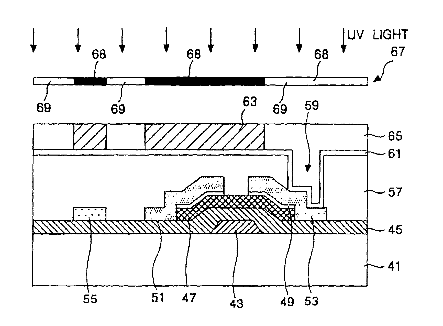
[0026]Reference will now be made in detail to the preferred embodiment of the present invention, an example of which is illustrated in the accompanying drawings.

[0027]Referring to FIG. 2A, aluminum (Al) or copper (Cu) is deposited on a transparent substrate 41, such as by sputtering technique or electroless plating, to form a metal thin film. A glass, a quartz, or a transparent plastic may be used for the transparent substrate 41. Then, the metal thin film is patterned to remain only at a desired portion of the transparent substrate 41 to form a gate electrode 43 that is electrically connected to a gate line (not shown). Patterning is beneficially performed by photolithography using a wet method.

[0028]Referring to FIG. 2B, a gate insulating film 45, an active layer 47, and an ohmic contact layer 49 are sequentially formed on the transparent substrate 41, beneficially by chemical vapor deposition (CVD), so as to cover the gate electrode 43 and the gate line (which is not shown). The ...


PUM

PropertyMeasurementUnit
temperatureaaaaaaaaaa
thicknessaaaaaaaaaa
temperatureaaaaaaaaaa

Abstract

A method of fabricating a liquid crystal display using a negative photo-resist. A passivation layer covering a thin film transistor, a data line, and a gate line is formed on a transparent substrate. The passivation layer is patterned to define a contact hole that exposes a drain electrode. A transparent conductive film in electrical contact with the drain electrode via the contact hole is then formed on the passivation layer. A negative-type photoresist is coated on the transparent conductive film. The transparent conductive film is then exposed with an image of the desired pixel electrode. The negative-type photoresist is then developed to expose portions of the transparent conductive film over a data line, a gate line, and the area of the thin film transistor area. The exposed transparent conductive film is then etched.

Description

[0001]This application claims the benefit of Korean Patent Application No. 2000-08307, filed on Feb. 21, 2000, which is hereby incorporated by reference for all purposes as if fully set forth herein.BACKGROUND OF THE INVENTION[0002]1. Field of the Invention[0003]The present invention relates to a liquid crystal display, and more particularly, to a method of fabricating a liquid crystal display (LCD) for preventing an electrical short.[0004]2. Discussion of the Related Art[0005]Generally, a liquid crystal display (LCD) includes switching devices consisting of thin film transistors, each having a gate electrode, a gate insulating film, an active layer, an ohmic contact layer, and source and drain electrodes. Liquid crystal is injected between a lower plate provided with pixel electrodes and an upper plate provided with color filters.[0006]In the LCD, N×M unit pixels (wherein N and M are integers), each of which includes a thin film transistor as a switching device and a pixel electrod...

Claims


Application Information

Patent Timeline
Patent Type & Authority Patents(United States)
IPC IPC(8): G02F1/13G02F1/1343G02F1/136G02F1/1362
CPCG02F1/136227G02F1/134336G02F2201/123B60T13/26B60T17/06B60Y2306/05
Inventor PARK, DUG JINPARK, HAI SUNGAHN, BYUNG CHUL
Owner LG DISPLAY CO LTD
Why Eureka
Try Eureka