Low power circuits with small voltage swing transmission, voltage regeneration, and wide bandwidth architecture

a low-power circuit and voltage-swing technology, applied in the field of integrated circuits, can solve the problems of high-performance integrated circuits, high power consumption, high data bandwidth at high transfer rate, and high power consumption, and achieve the effects of small swing operation, low power design, and reduced active fcv2 bus power

Active Publication Date: 2006-02-14
TAHOE RES LTD
View PDF4 Cites 12 Cited by
  • Summary
  • Abstract
  • Description
  • Claims
  • Application Information

AI Technical Summary

Benefits of technology

[0006]An exemplary embodiment of this invention presents a low power design to reduce the active fCV2 bus power by about 50–75%. Higher reduction occurs if two separate power sources are used. The lower limits of power reduction apply if single power source and voltage regulator are used to generate the two voltage sources needed for the low power, low voltage swing scheme. It is achieved by devising a small voltage swing scheme on the major data and control buses. The voltage signals on these interconnects swing only a portion of their traditional full swing values, in the range of approximately 50% of the full swing. An exemplary embodiment of this invention also introduces circuits and associated architectures that make the small swing operations possible and take advantage of them. These schemes involve single ended data-line structure, read and write data-lines, and regeneration circuits for data input / output (I / O) and for writing to the cells. The low voltage swing design also enables good, almost-digital, direct primary and secondary sensing, resulting in clean signal margins. An exemplary embodiment of this invention does not require the use of current sources in secondary sensing, and it has reduced susceptibility to voltage, temperature, and process (VTP) variations.
[0013]Accordingly, it is an object of an exemplary embodiment of this invention to teach low power high performance integrated circuits with high data bandwidths, achieved by reduced voltage swings on signal lines.

Problems solved by technology

Part of the problems is that the high speed of newer integrated circuits results in high power consumption.
Each simultaneously transmitted data is ultimately a voltage on an interconnection line, leading to dynamic, or active, power consumption.
The problem is that high throughput processors, comprising high performance integrated circuits, need wide data bandwidth at high transfer rates, and consume too much power.
Embedded memory macros, whether they are Static Random Access Memories (SRAM), or Dynamic Random Access Memories (DRAM), have inherently high dynamic, or active, power consumption due to high speed and high bandwidth.
Reducing speed or bandwidth would result in power saving, but to the detriment of processor performance.

Method used


Image

  • Low power circuits with small voltage swing transmission, voltage regeneration, and wide bandwidth architecture
  • Low power circuits with small voltage swing transmission, voltage regeneration, and wide bandwidth architecture
  • Low power circuits with small voltage swing transmission, voltage regeneration, and wide bandwidth architecture

Examples


Embodiment Construction

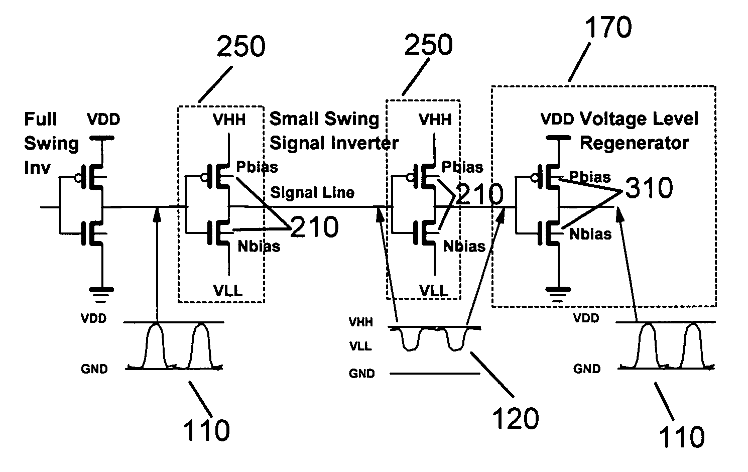
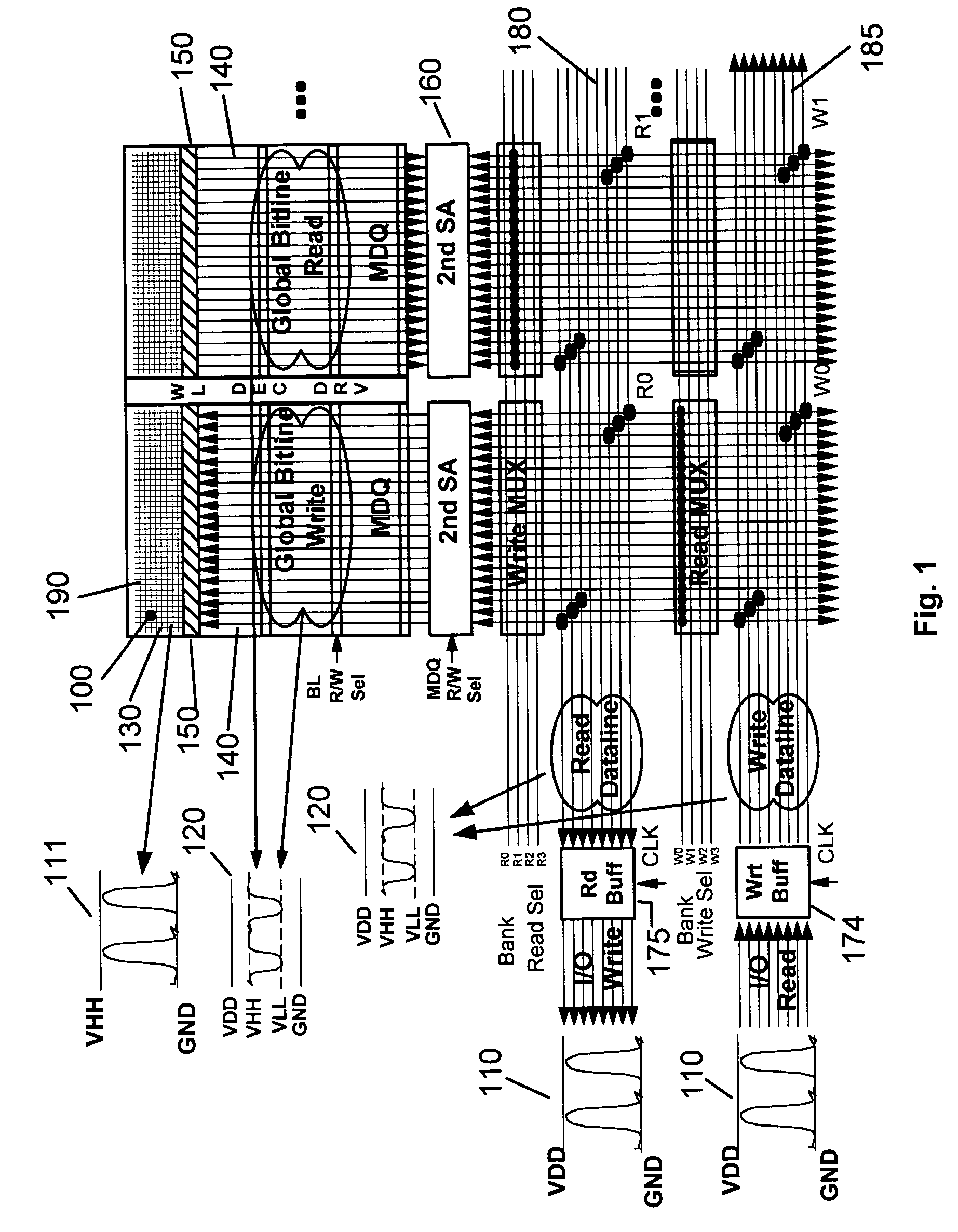
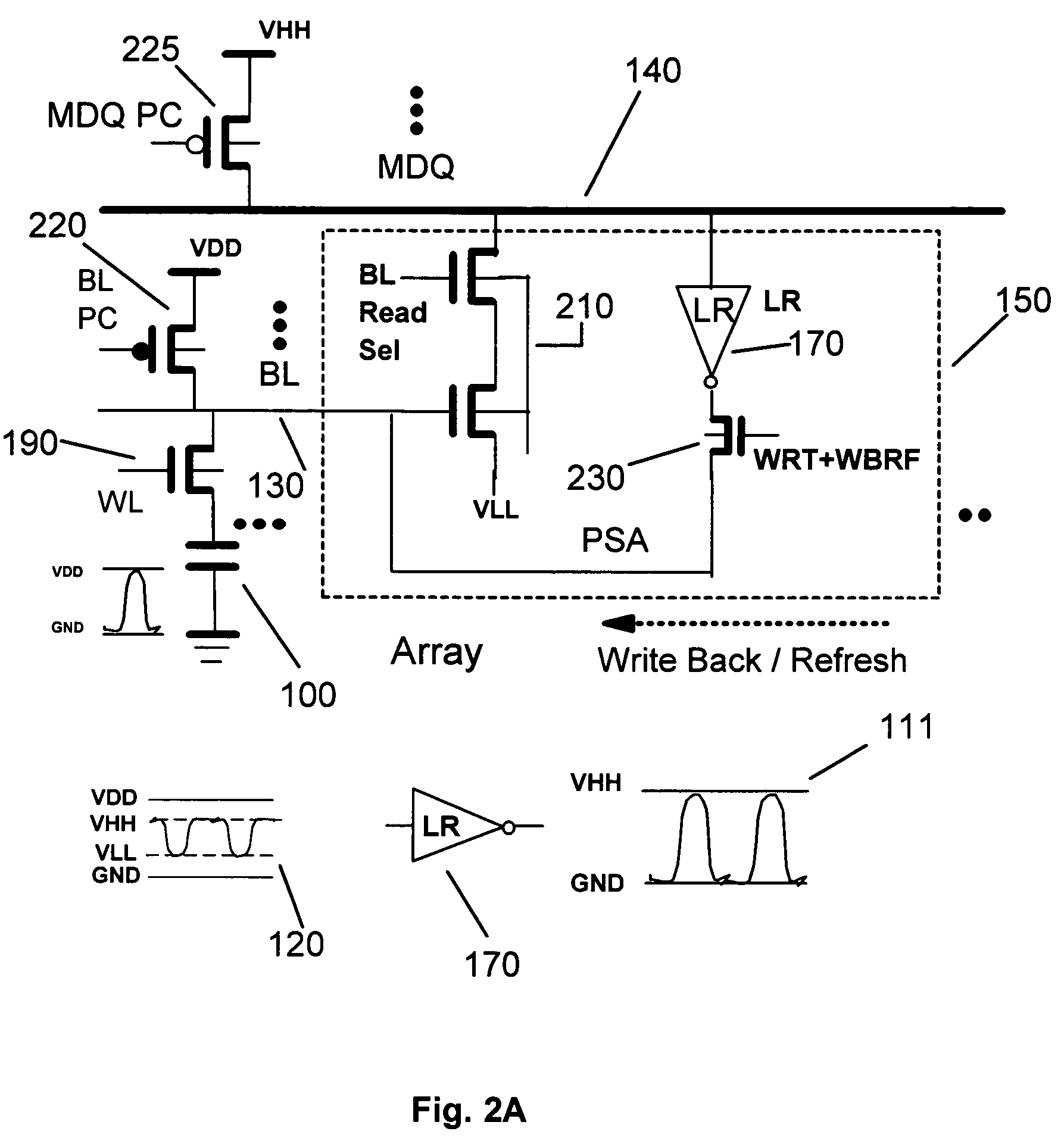
[0027]An embedded memory macro, such as a DRAM or SRAM macro, is an embodiment of an inherently high bandwidth, high dynamic power consumption integrated circuit. In the disclosed design such a macro has an architecture in which specific signal lines, such as a global data-bus, have a voltage swing which is limited to a portion of the bitline supply voltage during the Read / Write operations. On the other hand, in a DRAM for the reason of maintaining enough signal margin during a Read operation and to have sufficient retention time, full bitline voltage has to be written to a DRAM cell. At the other end of the global data-bus, which is the I / O interface to the external logic, the full voltage of the external logic is interfaced with the reduced voltage of the global data-bus.

[0028]FIG. 1 shows a schematic of a small swing DRAM macro architecture, as an embodiment of an integrated circuit with lowered power consumption. The DRAM cells 100 are at the crossings of bitlines 130 and a word...


PUM


Abstract

An integrated circuit, such as a memory macro, includes multiple power rails supporting first and second voltage differentials, with the second voltage differential being smaller than the first voltage differential. Signal lines in the integrated circuit are driven with the small voltage swing, which is generated by small swing circuits. The integrated circuit further includes regeneration circuits, which are receiving small voltage swing inputs and are outputting first, or full voltage swings. The application of the small voltage swing to the signal lines saves power in the integrated circuit. A wide bandwidth, full-wordline I / O, memory integrated circuit has simultaneously operable connection paths between essentially all the memory cells that are attached to the same wordline and the corresponding I / O terminals, and it has a single ended data-line structure.

Description

FIELD OF THE INVENTION[0001]The present invention relates to integrated circuits that have high data throughput rates. In particular, an exemplary embodiment of this invention deals with power saving measures involving reduced voltage swings on signal lines, and a wide bandwidth architecture.BACKGROUND OF THE INVENTION[0002]Today's integrated circuits include a vast number of transistor devices formed in a semiconductor. Smaller devices are the key to enhance performance and to increase reliability. As devices are scaled down, however, the technology becomes more complex and new methods are needed to maintain the expected performance enhancement from one generation of devices to the next.SUMMARY OF THE INVENTION[0003]Part of the problems is that the high speed of newer integrated circuits results in high power consumption. In CMOS circuits significant fraction of power consumption is the result of dynamic, or active, power. Dynamic power is consumed when capacitors are charged and d...

Claims


Application Information

Patent Timeline
Patent Type & Authority Patents(United States)
IPC IPC(8): G11C7/00G11C5/06G11C11/406G11C11/4074
CPCG11C5/063G11C11/4074G11C11/406G11C2207/104
Inventor LUK, WING K.DENNARD, ROBERT H.KOSONOCKY, STEPHEN V.
Owner TAHOE RES LTD
Why Eureka
Try Eureka