Low power circuits with small voltage swing transmission, voltage regeneration, and wide bandwidth architecture

Active Publication Date: 2005-02-10
TAHOE RES LTD
View PDF4 Cites 10 Cited by
  • Summary
  • Abstract
  • Description
  • Claims
  • Application Information

AI Technical Summary

Benefits of technology

Accordingly, it is an object of an exemplary embodiment of this invention to teach low power high perfor

Problems solved by technology

Part of the problems is that the high speed of newer integrated circuits results in high power consumption.
Each simultaneously transmitted data is ultimately a voltage on an interconnection line, leading to dynamic, or active, power consumption.
The problem is that high throughput processors, comprising high performance integrated circuits, need wide data bandwidth at

Method used


Image

  • Low power circuits with small voltage swing transmission, voltage regeneration, and wide bandwidth architecture
  • Low power circuits with small voltage swing transmission, voltage regeneration, and wide bandwidth architecture
  • Low power circuits with small voltage swing transmission, voltage regeneration, and wide bandwidth architecture

Examples


Embodiment Construction

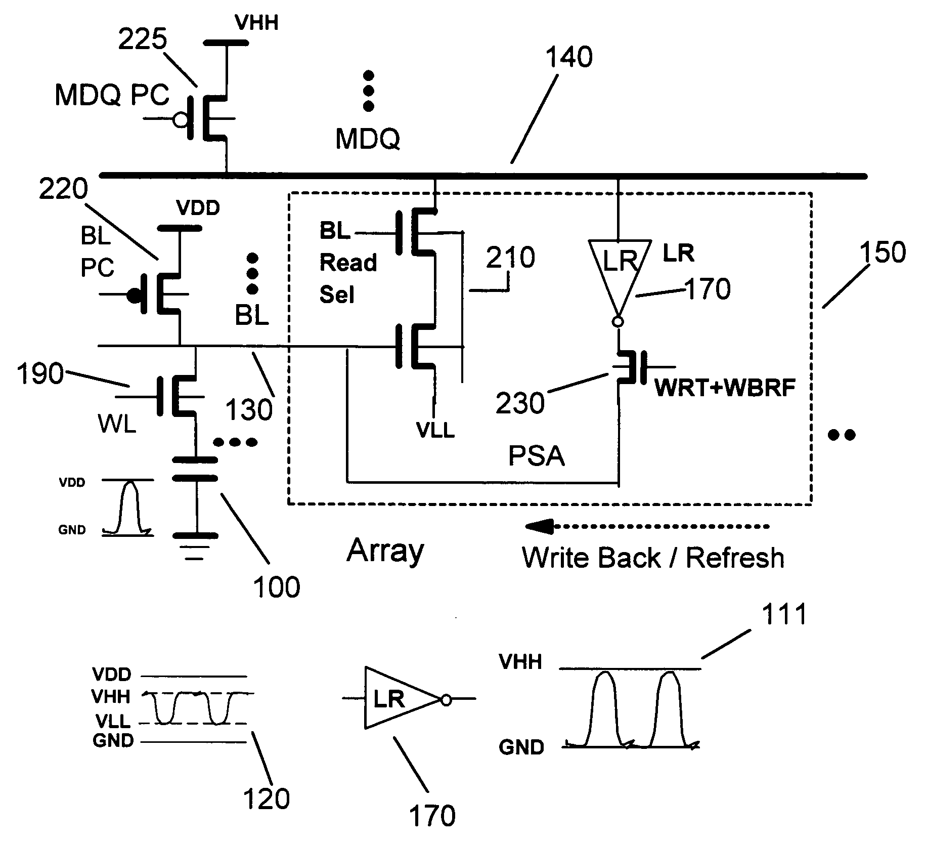
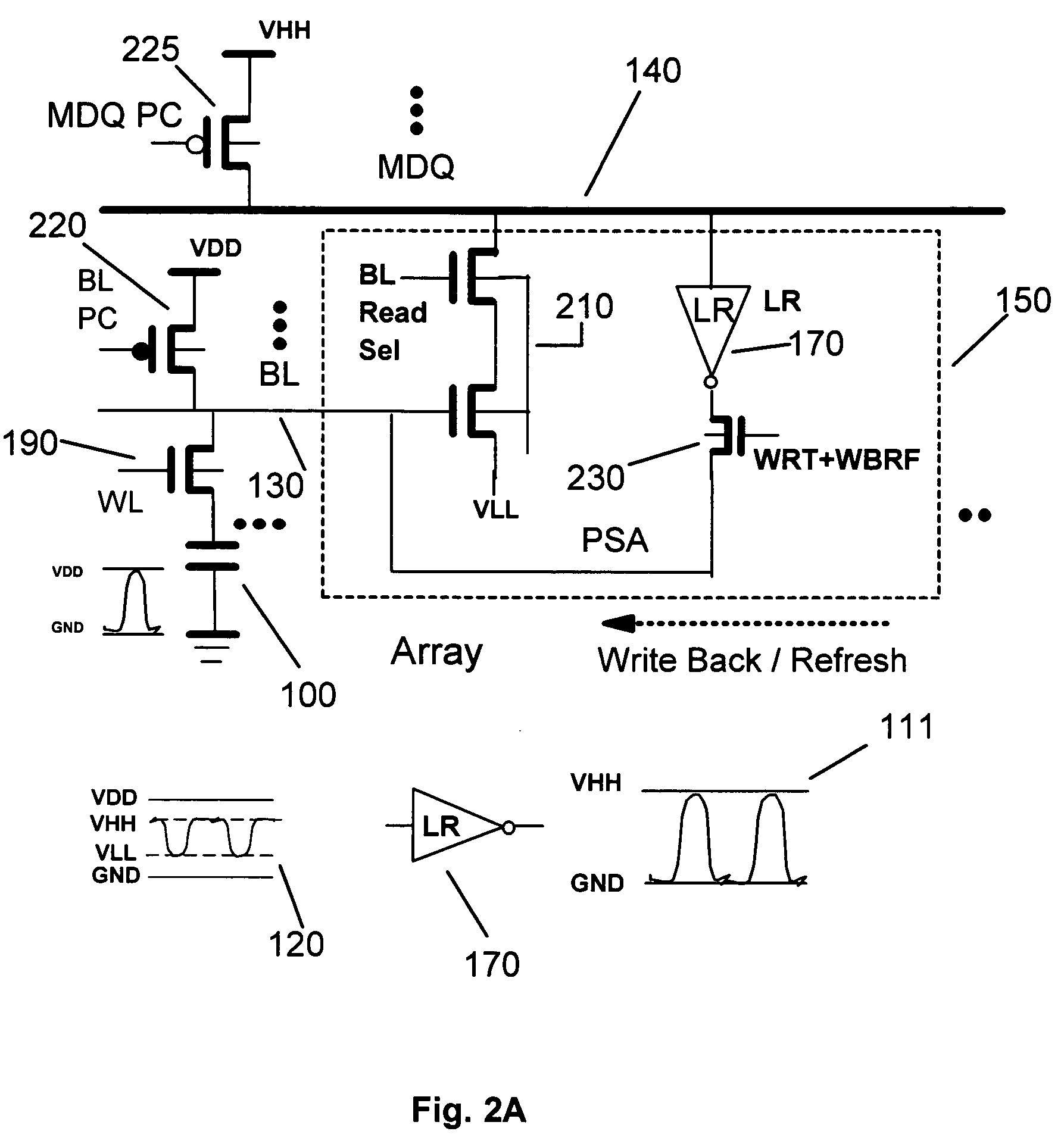
An embedded memory macro, such as a DRAM or SRAM macro, is an embodiment of an inherently high bandwidth, high dynamic power consumption integrated circuit. In the disclosed design such a macro has an architecture in which specific signal lines, such as a global data-bus, have a voltage swing which is limited to a portion of the bitline supply voltage during the Read / Write operations. On the other hand, in a DRAM for the reason of maintaining enough signal margin during a Read operation and to have sufficient retention time, full bitline voltage has to be written to a DRAM cell. At the other end of the global data-bus, which is the I / O interface to the external logic, the full voltage of the external logic is interfaced with the reduced voltage of the global data-bus.

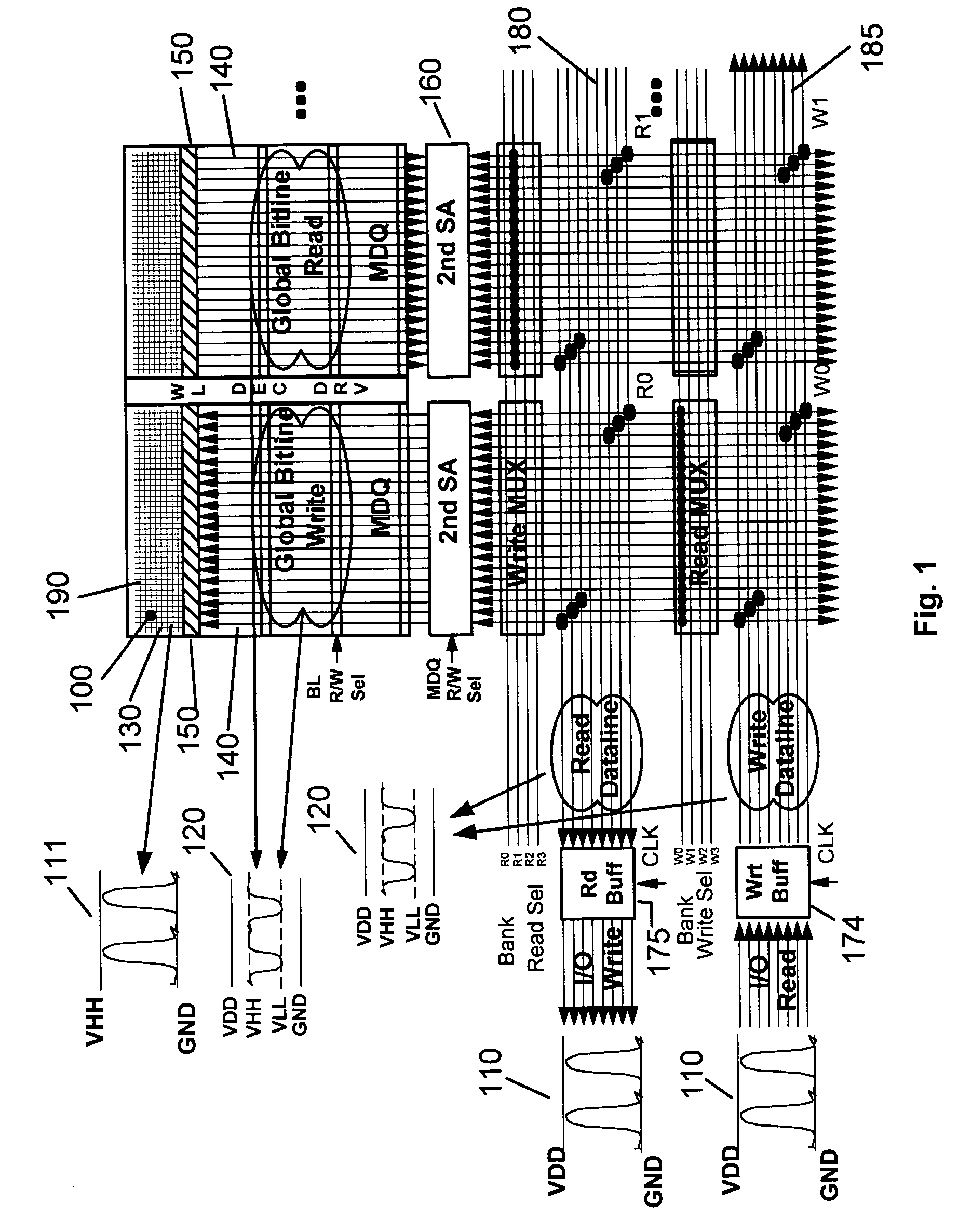
FIG. 1 shows a schematic of a small swing DRAM macro architecture, as an embodiment of an integrated circuit with lowered power consumption. The DRAM cells 100 are at the crossings of bitlines 130 and a wordlines 190....


PUM


Abstract

An integrated circuit, such as a memory macro, includes multiple power rails supporting first and second voltage differentials, with the second voltage differential being smaller than the first voltage differential. Signal lines in the integrated circuit are driven with the small voltage swing, which is generated by small swing circuits. The integrated circuit further includes regeneration circuits, which are receiving small voltage swing inputs and are outputting first, or full voltage swings. The application of the small voltage swing to the signal lines saves power in the integrated circuit. A wide bandwidth, full-wordline I/O, memory integrated circuit has simultaneously operable connection paths between essentially all the memory cells that are attached to the same wordline and the corresponding I/O terminals, and it has a single ended data-line structure.

Description

FIELD OF THE INVENTION The present invention relates to integrated circuits that have high data throughput rates. In particular, an exemplary embodiment of this invention deals with power saving measures involving reduced voltage swings on signal lines, and a wide bandwidth architecture. BACKGROUND OF THE INVENTION Today's integrated circuits include a vast number of transistor devices formed in a semiconductor. Smaller devices are the key to enhance performance and to increase reliability. As devices are scaled down, however, the technology becomes more complex and new methods are needed to maintain the expected performance enhancement from one generation of devices to the next. SUMMARY OF THE INVENTION Part of the problems is that the high speed of newer integrated circuits results in high power consumption. In CMOS circuits significant fraction of power consumption is the result of dynamic, or active, power. Dynamic power is consumed when capacitors are charged and discharged....

Claims


Application Information

Patent Timeline
IPC IPC(8): G11C5/06G11C11/406G11C11/4074
CPCG11C5/063G11C2207/104G11C11/4074G11C11/406
Inventor LUK, WING K.DENNARD, ROBERT H.KOSONOCKY, STEPHEN V.
Owner TAHOE RES LTD
Why Eureka
Try Eureka