
Optical switches made by nematic liquid crystal switchable mirrors, and apparatus of manufacture

a technology of liquid crystal switchable mirrors and optical switches, applied in the field of optical matrix switches, can solve the problems of narrow spectral bandwidth, low device reflectivity, and significant polarization dispersion loss

Inactive Publication Date: 2006-02-14
KENT OPTRONICS
View PDF17 Cites 95 Cited by
  • Summary
  • Abstract
  • Description
  • Claims
  • Application Information

AI Technical Summary

Benefits of technology

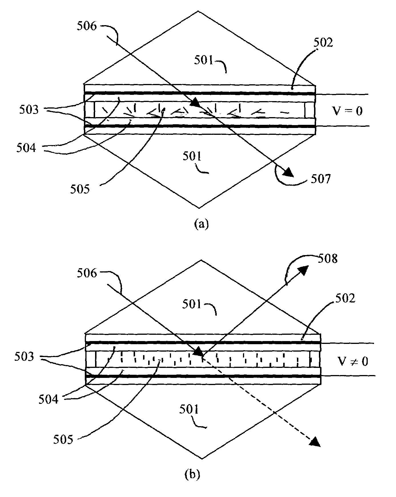
[0017]The present invention describes a new electrically switchable apparatus made by liquid crystal, switch matrix constructed by the switchable apparatus and the methods for manufacturing the switch matrix. The switching mechanism is based on the electrically induced refractive index change of a liquid crystal material, which further causes an incident light on the liquid crystal interface to be either totally reflected or transmitted regardless of the light polarization state. In one state, the liquid crystal is set in the isotropic phase in the absence of an electric field with a refractive index nISO=[(ne2+2no2)/3]1/2, where no and ne are ordinary and extraordinary refractive index of the liquid crystal, respectively. nISO is larger than no but smaller than ne. If nISO of the liquid crystal is chosen to match that of the surrounding medium such as a glass substrate, all the polarization components of the light are transmitted since nISO is optically isotropic. In another state w

Problems solved by technology

Furthermore, the optical modulation by the liquid crystal phase shifter or rotator is intrinsically not broadband, which imposes significant optical cross talk at the wavelengths outside the liquid crystal device bandwidth.
Finally, this technology intrinsically is polarization dependent and has significant polarization dispersion loss (PDL).
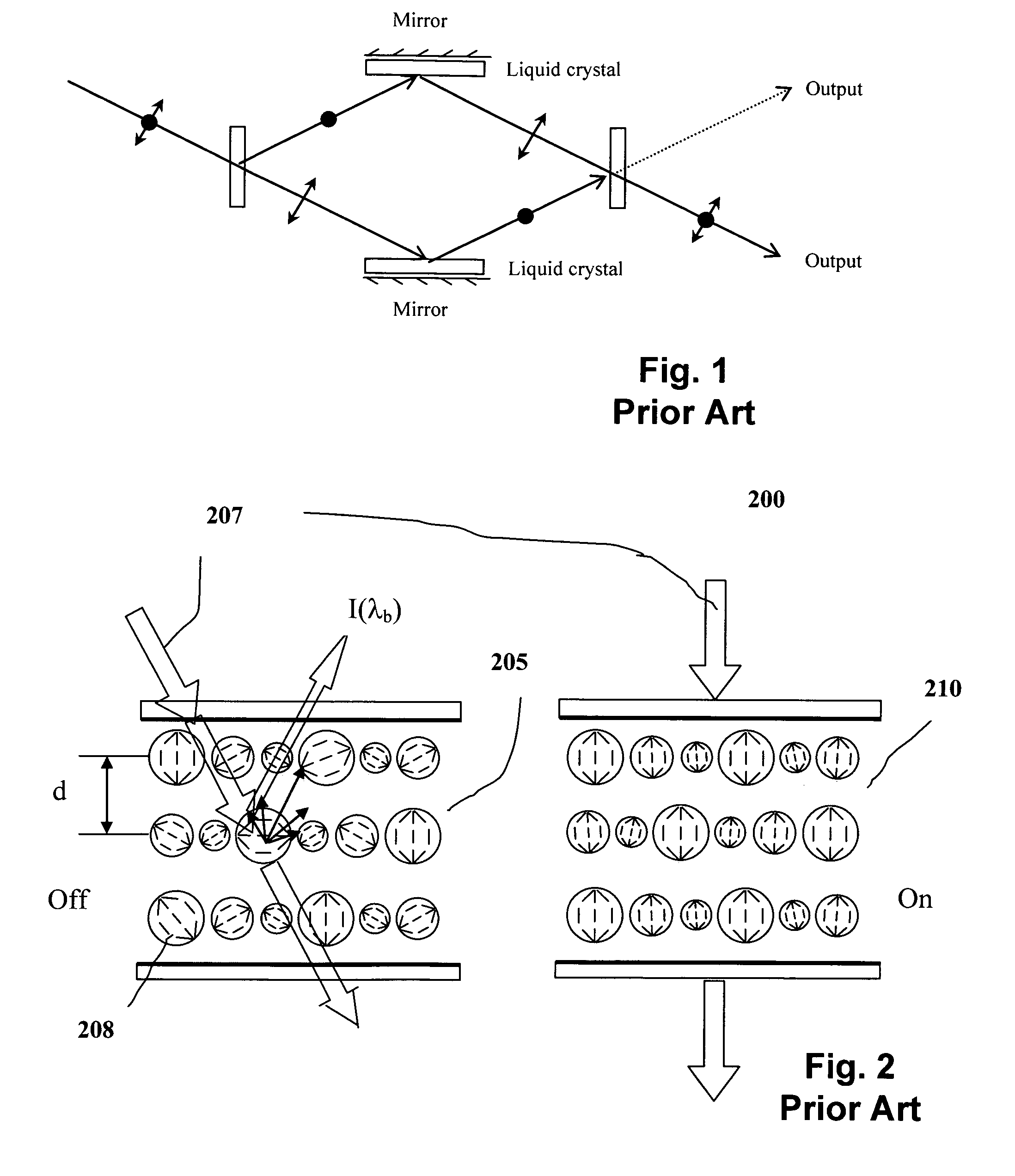
However, the device shows a very low reflectivity (only around 50% or less) and its spectral bandwidth is narrow (only around 30 nm).
The displacement of the two reflected beams becomes more pronounced when the incoming light is incident at a large angle, which makes this apparatus less desirable for building a switch for optical communication than the other aforementioned apparatuss.
However, it still needs two layers of CLC's with opposite handedness for operation under an unpolarized light.

Method used


Image

  • Optical switches made by nematic liquid crystal switchable mirrors, and apparatus of manufacture
  • Optical switches made by nematic liquid crystal switchable mirrors, and apparatus of manufacture
  • Optical switches made by nematic liquid crystal switchable mirrors, and apparatus of manufacture

Examples


first embodiment

[0056]The first embodiment describes the single layer switchable element made by a liquid crystal. The exemplary liquid crystal is a nematic liquid crystal with either positive dielectric anisotropy (Δε>0) or negative dielectric anisotropy (Δε<0) although other liquid crystals are applicable.

A. Free Space Switchable Elements

[0057]a. Switchable Element with Conventional Electrodes—I

[0058]FIG. 5 shows the first switchable element structure, in which the liquid crystal (505) is sandwiched between two substrates (502) with Indium Tin Oxide (ITO) electrode (503). The liquid crystal is a nematic liquid crystal with a positive dielectric anisotropy (Δε≧0). The ITO electrodes (503) are within the optical path of the incident beam (506), transmitted beam (507) and reflected beam (508). Between the ITO and the liquid crystal, there is an index matching layer (504). Two optical coupling elements such as prisms (501) are attached to the apparatus. It is preferred that the coupling elements have...

third embodiment

[0108]The following is the third embodiment related to the fabrication procedure for the optical switch array.

(a) Fabrication Procedure for Free Space (Non-Waveguide) Switch Array

[0109]The following fabrication method is described for constructing the free space cross connect optical switch array as shown in FIG. 21. First individual empty liquid crystal cells 2300 are assembled, as shown in FIG. 23. While each cell has the structure as shown by the four pairs of electrodes 2305, this number has been selected only for illustration purposes and does not limit the number of electrodes which could be fewer than four, or any number larger than the electrodes are arranged on substrate 2310. If a positive liquid crystal is used, the pixilated ITO electrodes are patterned into the comb-like structure for in-plane switching which are located on only one substrate surface.

[0110]The empty cells are then stacked, aligned to a proper position to each other and fixed to each other using the simi...


PUM

PropertyMeasurementUnit
Temperatureaaaaaaaaaa
Magnetic fieldaaaaaaaaaa
Transparencyaaaaaaaaaa

Abstract

Technology for constructing a single layer polarization insensitive electrically switchable liquid crystal mirror is disclosed which serves as the basic element for constructing an optical router switch array in free space as well as waveguide format. The optical router switch array includes a plurality of switchable liquid crystal mirror elements having liquid crystal arranged in stack cells and / or in a waveguide configuration. The resulted optical router switches are motionless, polarization insensitive, stable within the operational spectral region, and stable versus temperature. The invention also includes methods for manufacturing a single switchable liquid crystal mirror element and the optical switch arrays. The same technology is further extended to constructing an electrically tunable optical filter that is motionless and polarization insensitive.

Description

[0001]This application claims priority from U.S. provisional application 60 / 335,074 filed on Oct. 26, 2001.BACKGROUND OF THE INVENTION[0002]1. Field of the Invention[0003]The present invention relates to optical matrix switches made by single layer liquid crystal switchable elements and the fabrication methods.[0004]2. Description of the Related Art[0005]High performance optical matrix switches are critical components for telecom. Quality switchable mirrors are important in constructing the high performance optical matrix switches. In the following, related prior art technologies are cited as the reference for the present invention. The first prior art technology is based on liquid crystal phase shifter / rotator as disclosed by, Corning, Exhibition in NFOEC'2000, Denver, Colo., Aug. 27–31, 2000 and SpectraSwitch, Exhibition in NFOEC'2000, Denver, Colo., Aug. 27–Aug. 31, 2000 and Chorum, Exhibition in NFOEC'2000, Denver, Colo., Aug. 27–Aug. 31, 2000. This technology switches light wit...

Claims


Application Information

Patent Timeline
IPC IPC(8): G02B6/26
CPCG02F1/07G02F1/1326G02F1/137G02F1/31G02F1/315G02F1/1334G02B6/351G02B6/3546G02F2001/213G02F1/213
Inventor CHEN, ZHANLI, LE
Owner KENT OPTRONICS
Learn More