Linear low noise transconductance cell

a transconductance cell, low noise technology, applied in the field of amplifiers, can solve the problems of insufficient linearity of analog signal processing circuits, insufficient linearity of transconductance cells, and high cost of linearity and transconductance improvement, and achieve low noise, improve linearity, and improve linearity.

Inactive Publication Date: 2006-02-21
AVAGO TECH WIRELESS IP SINGAPORE PTE
View PDF9 Cites 11 Cited by
  • Summary
  • Abstract
  • Description
  • Claims
  • Application Information

AI Technical Summary

Benefits of technology

[0008]In accordance with aspects of the present invention, a transconductance cell includes resistance stage coupled between two equivalent half circuits. Each half-circuit includes a feedback loop. In the feedback loop the drain of the input differential transistor is coupled to the input of the inverting gain stage. The output of the inverting gain stage is coupled to the gate of the output differential transistor. The source of the output differential transistor is coupled to the source of the input transistor. The resistance stage is coupled to the source of the input transistor in each feedback loop. In an aspect of the present invention, the resistance stage includes a resistor. In another aspect of the present invention, the resistance stage includes a plurality of resistors.
[0009]In accordance with aspects of the present invention, a low noise transconductance cell includes a bias current source coupled between a first circuit node (e.g., VDD) and a differential circuit pair having two equivalent half circuits. The low noise transconductance cell also includes an optional load current stage having two or more current sources. Each half-circuit includes a feedback loop coupled to a resistor. The resistor in the first half-circuit is coupled in series to the resistor in the second half circuit. The current source is connected to a first circuit node and a node between the two resistors. In the feedback loop the drain of the input differential transistor is coupled to the input of the inverting gain stage. The output of the inverting gain stage is coupled to the gate of the output differential transistor. The source of the output differential transistor is coupled to the source of the input transistor. In each feedback loop, the drain of the input transistor is coupled to a current source in the load current stage. In accordance with another aspect of the present invention, the drain of the output transistor is coupled to a current source in the load current stage.
[0010]In accordance with aspects of the present invention, high swing transconductance cell includes differential circuit pair having two equivalent half circuits. High swing transconductance cell also includes a load current stage having two or more current sources. Each half-circuit includes a feedback loop coupled to a resistor. The resistor in the first half-circuit is coupled in series to the resistor in the second half circuit. The high swing cell further includes two bias current sources. The first bias current source is connected to the left terminal of the series connected resistors and the second bias current source is connected to the right terminal of the series connected resistors. In accordance with another aspect of the present invention, a single resistor is used in place of two series connected resistors. In the feedback loop the drain of the input differential transistor is coupled to the input of the inverting gain stage. The output of the inverting gain stage is coupled to the gate of the output differential transistor. The source of the output differential transistor is coupled to the source of the input transistor. In each feedback loop, the drain of the input transistor is coupled to a current source in the load current stage. In accordance with another aspect of the present invention, the drain of the output transistor is coupled to a current source in the load current stage.
[0011]In accordance with aspects of the present invention, the low noise transconductance cell has improved linearity and optionally programmable resistance. Low noise transconductance cell includes two equivalent feedback loops. In each feedback loop, the drain of the input transistor is coupled to the negative input of the amplifier. A floating voltage source is coupled between the source of the input transistor and the positive terminal of the amplifier. The output of the amplifier is coupled to the gate of the output transistor. In accordance with another aspect of the present invention, the low noise transconductance cell includes a plurality of resistance stages that can be coupled between the feedback loops, as needed.
[0012]In accordance with aspects of the present invention, transconductance cell includes two equivalent feedback loops, a first resistance stage, and a second resistance stage. When the first resistance stage is needed, switches couple the first resistance stage between the first and second feedback loops. When the second resistance stage is needed, switches couple the second resistance stage between the first and second feedback loops. In accordance with another aspect of the present invention, when the first resistance stage is needed, first and second current sources are coupled, via switches, to a circuit node (e.g., supply voltage) and to a node between the first and second resistors of the first resistance stage. This makes the transconductance cell operate as a low noise transconductance cell. When the second resistance stage is needed, the first current source is coupled to first end of the second resistance stage and the second current source is coupled, via switches, to the second end of the second resistance stage. This makes the transconductance cell operate as a high swing transconductance cell.
[0013]In accordance with aspects of the present invention, an analog circuit includes a low noise transconductance cell, a high swing transconductance cell, and an output switch. In an aspect of the invention, the analog circuit may also include an input switch. When a low noise transconductance cell is required, the input switch couples the differential inputs of the switch to the differential inputs of the low noise transconductance cell. The output switch couples the differential outputs of the low noise transconductance cell to the inputs of the next circuit component. When a high swing transconductance cell is required, the input switch couples the differential inputs of the switch to the differential inputs of the high swing transconductance cell. The output switch couples the differential outputs of the low gain transconductance cell to the inputs of the next circuit component.

Problems solved by technology

As a result, the linearity of the analog signal processing circuit is limited.
Consequently, the gain of the transconductance cell is not accurate.
However, these improvements in linearity and transconductance are expensive.

Method used


Image

  • Linear low noise transconductance cell
  • Linear low noise transconductance cell
  • Linear low noise transconductance cell

Examples


Embodiment Construction

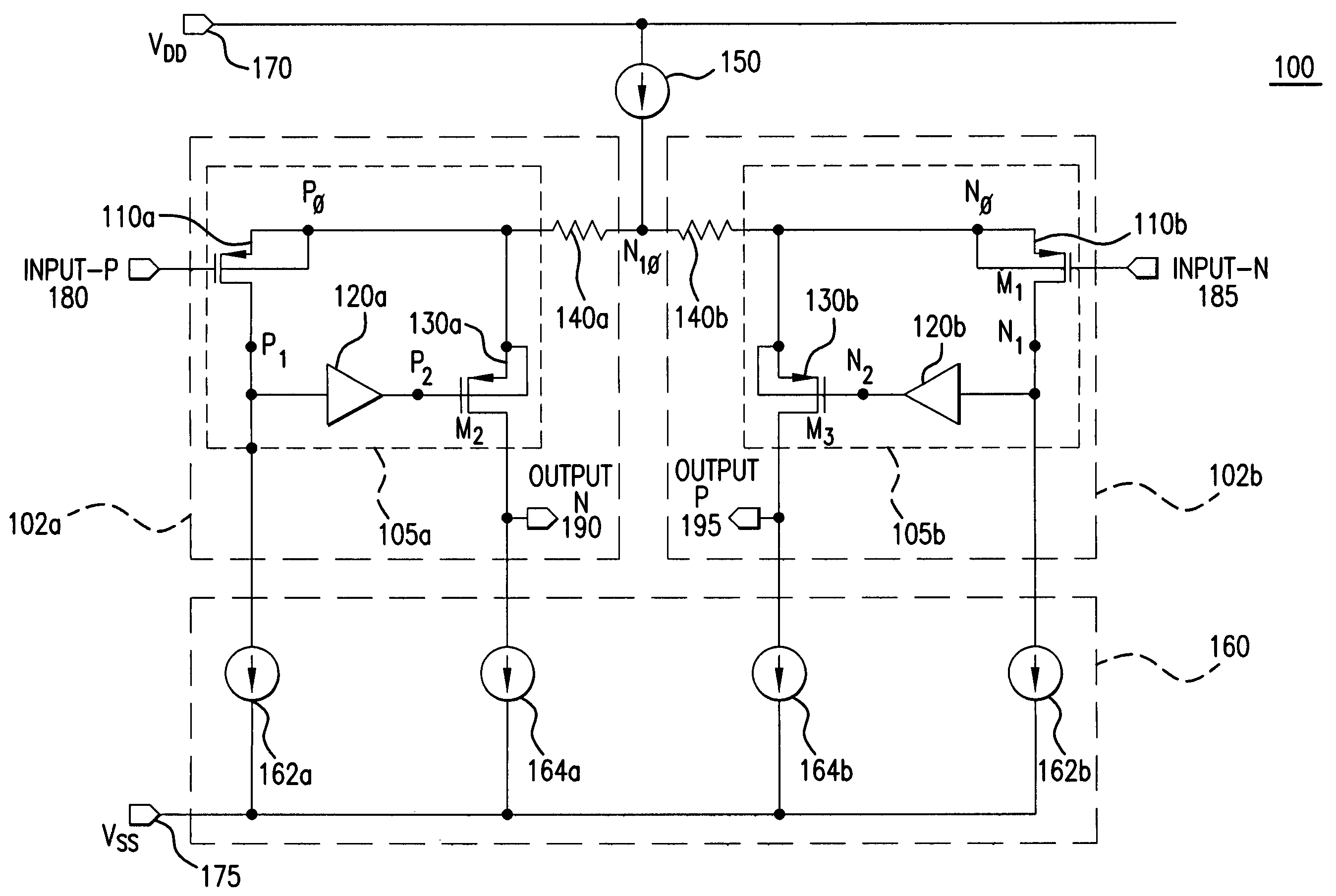
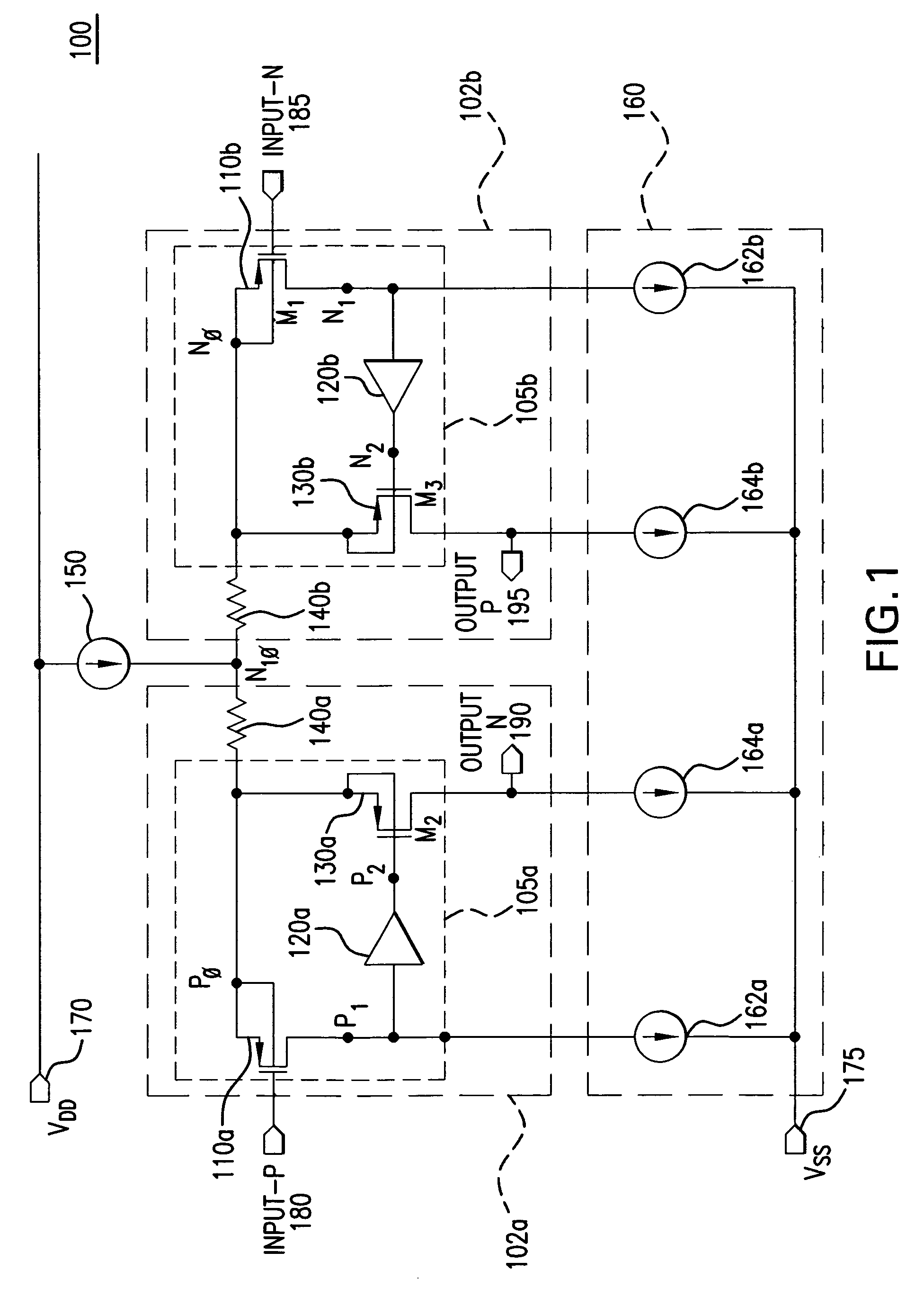
[0026]FIG. 1 is a block diagram of a low noise transconductance cell 100, according to an embodiment of the present invention. Transconductance cell 100 is connected between supply potential VDD 170 and supply potential VSS 175. In operation, transconductance cell 100 is operably coupled to receive a differential input voltage at input-p 180 and input-n 185. Transconductance cell 100 then converts the differential input voltage into a differential output current at output-n 190 and output-p 195.

[0027]Transconductance cell 100 includes a differential circuit pair having two equivalent half-circuits 102a and 102b, a bias current source 150, and a load current stage 160. The dimensions and values of the components in each half-circuit are matched to create the balanced differential circuit.

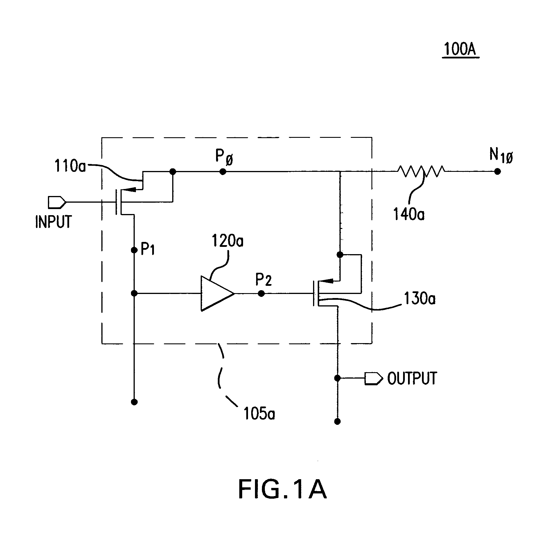
[0028]Each half-circuit 102a, 102b includes a feedback loop 105a, 105b. In an embodiment of the present invention, each half-circuit 102a, 102b also includes a resistor 140a, 140b coupled to the feed...


PUM


Abstract

A low noise transconductance cell includes a resistor and a differential circuit pair having two equivalent half-circuits. Each half-circuit includes a feedback loop coupled to the resistor. The feedback loop includes an input transistor coupled to an inverting gain stage. The inverting gain stage is coupled to an output transistor which in turn is coupled to the input transistor and the resistor. In a low noise transconductance cell, a bias current source is coupled to the center of series connected resistors. In a high swing transconductance cell, a first bias current source is coupled to the left terminal of a resistance stage and a second bias current source is coupled to the right terminal of the resistance stage. The resistance stage can include a single resistor or a plurality of resistors.

Description

CROSS REFERENCE TO RELATED APPLICATIONS[0001]This application claims priority to U.S. Provisional Application No. 60 / 447,332, entitled “Microphone Preamplifier Circuit with Low Noise GM Transconductance Cell,” filed Feb. 14, 2003, which is incorporated herein by reference in its entirety.FIELD OF THE INVENTION[0002]The application relates generally to amplifiers and more particularly to transconductance cells.BACKGROUND OF THE INVENTION[0003]Analog signal processing is commonplace in a wide variety of low-power, low-cost applications such as mobile telephones, laptops, personal digital assistants (PDAs), hearing aids, etc. These applications usually require low noise, low power, and high performance circuits. In addition, these applications require low total harmonic distortion (THD) which is related to the linearity of the circuit. To achieve the desired operating characteristics, many of these signal processing applications use programmable gain amplifiers (PGAs) and analog filter...

Claims


Application Information

Patent Timeline
Patent Type & Authority Patents(United States)
IPC IPC(8): G06G7/12G06G7/26H03F3/45H03K5/22H03K5/24
CPCH03F3/45183H03K5/2481H03F2203/45352H03F2203/45356H03F2203/45392H03F2203/45504H03F2203/45648H03F2203/45696H03F2203/7203H03F2203/45396
Inventor BROOKS, TODDSONG, JUNGWOOTONG, WYNSTAN
Owner AVAGO TECH WIRELESS IP SINGAPORE PTE
Why Eureka
Try Eureka