Distributed feedback semiconductor laser device
a semiconductor laser and semiconductor technology, applied in the direction of lasers, semiconductoronductors, optical resonator shape and construction, etc., can solve the problems of reducing the light emitting strength of the p-type device, reducing the frequency response of the laser, so as to achieve the effect of small threshold current, excellent frequency characteristics, and small device resistan
- Summary
- Abstract
- Description
- Claims
- Application Information
AI Technical Summary
Benefits of technology
Problems solved by technology
Method used
Image
Examples
embodiment 1
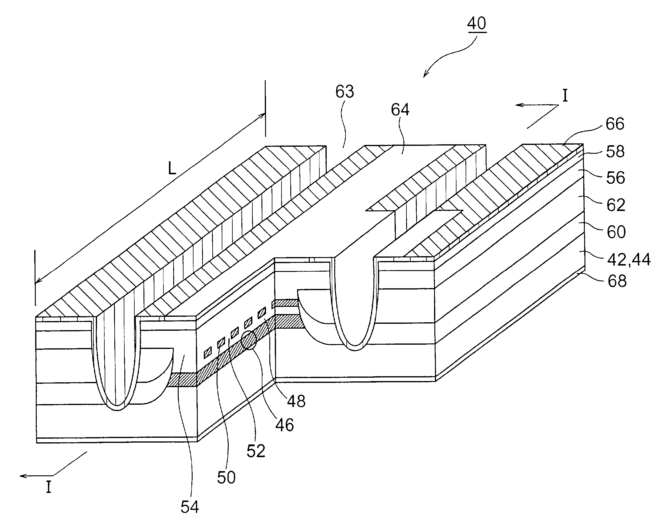
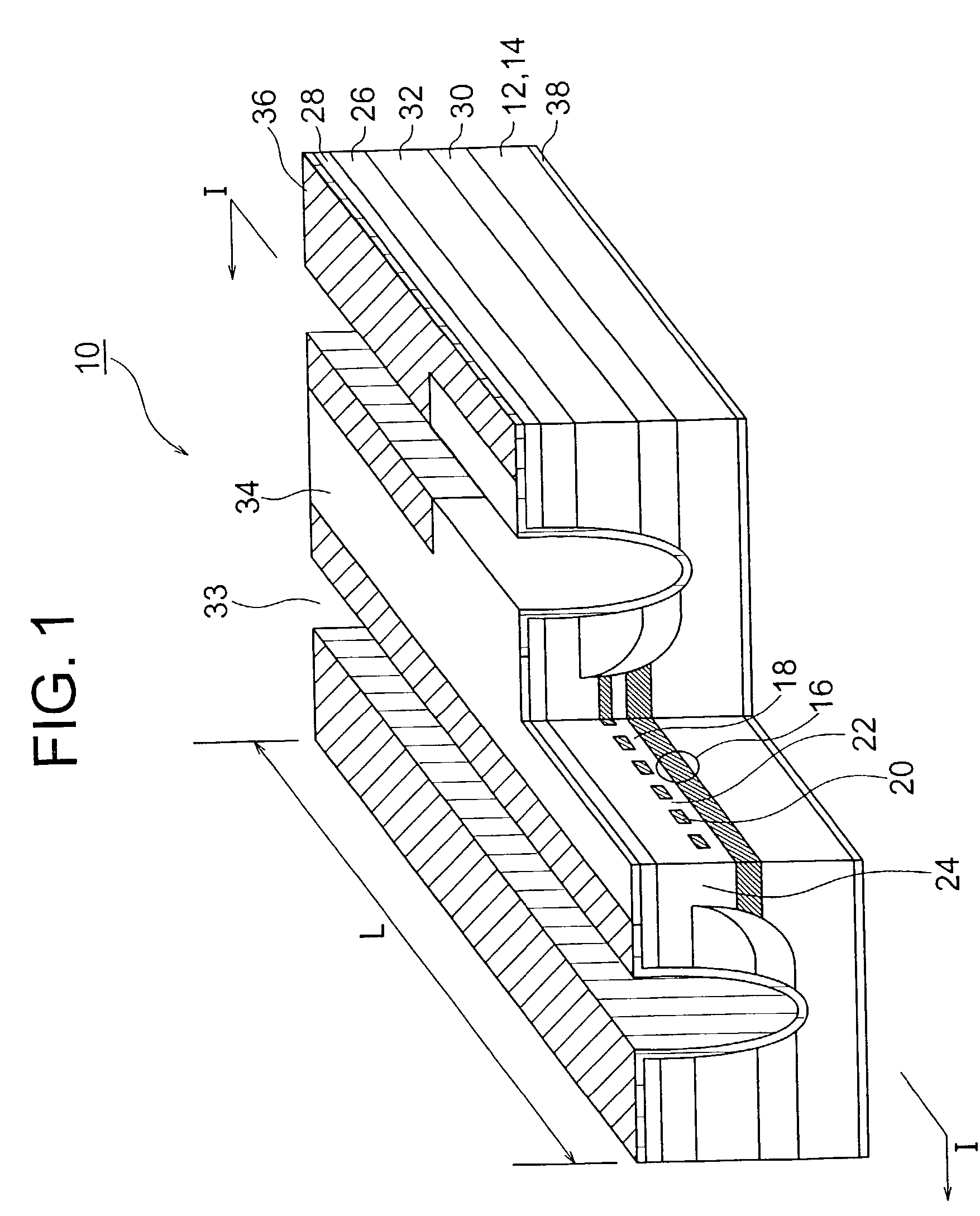
[0070]As shown in FIG. 7, a DFB laser 40 includes substantially the same configuration as the above test DFB laser 10 except that the carrier densities of InGaAsP diffraction gratings 50 and a p-InP embedding layer 52 are 1×1018 cm−3.
[0071]The DFB laser 40 is a BH type DFB laser having a cavity length (L) of 300 μm and a lasing wavelength of 1550 nm, and includes a layer structure on an n-InP semiconductor substrate 42 having thickness of about 350 μm. The layer structure includes an n-InP buffer layer 44, an MQW-SCH active layer 46, a P-InP spacer layer 48 having thickness of about 200 nm, the p-InP embedding layer 52 having therein the buried InGaAsP-diffraction gratings 50, and a p-InP top cladding layer 54.
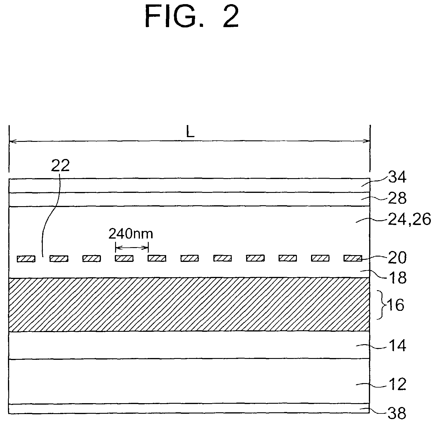
[0072]The bandgap of the MQW-SCH active layer 46 is 1550 nm when converted into the wavelength. The thickness of the diffraction grating layer is about 20 nm. The cycle of the diffraction grating 20 is about 240 nm and the duty ratio is about 30%. The carrier density of the In...
embodiment 2
[0087]A DFB laser 80 of the present embodiment includes substantially the same configuration as the above DFB laser 40 except that the lasing wavelength is 1310 nm, the cavity length (L) is 300 μm and the waveguide is the ridge-type.
[0088]As shown in FIG. 8, the DFB laser 80 has a layer structure, on an n-InP semiconductor substrate 78 having thickness of about 350 μm, including an n-InP buffer layer 69, an MQW-SCH active layer (InGaAsP) 70, a P-InP spacer layer 71, a p-InP embedding layer 73 having therein buried diffraction grating 72, and a p-InP cladding layer 74.
[0089]The material of the active layer is not restricted to the InGaAsP / InP, and AlGaInAs / InP can be used.
[0090]The bandgap of the MQW-SCH active layer 70 is 1335 nm when converted into the wavelength. The cycle of the diffraction grating 72 is about 200 nm and the duty ratio is about 30%.
[0091]The carrier densities of the compound semiconductor layer constituting the diffraction grating 72 and the embedding layer 73 ar...
PUM
 Abstract
Description
Claims
Application Information


