

Semiconductor laser device
a laser device and semiconductor technology, applied in semiconductor lasers, laser details, electrical devices, etc., can solve the problems of low reliability, increase the threshold current, reduce the optical confinement ratio within the active layer, etc., and achieve high efficiency, small operating current, and high reliability.
- Summary
- Abstract
- Description
- Claims
- Application Information
AI Technical Summary
Benefits of technology
Problems solved by technology
Method used
Image

Examples
first embodiment
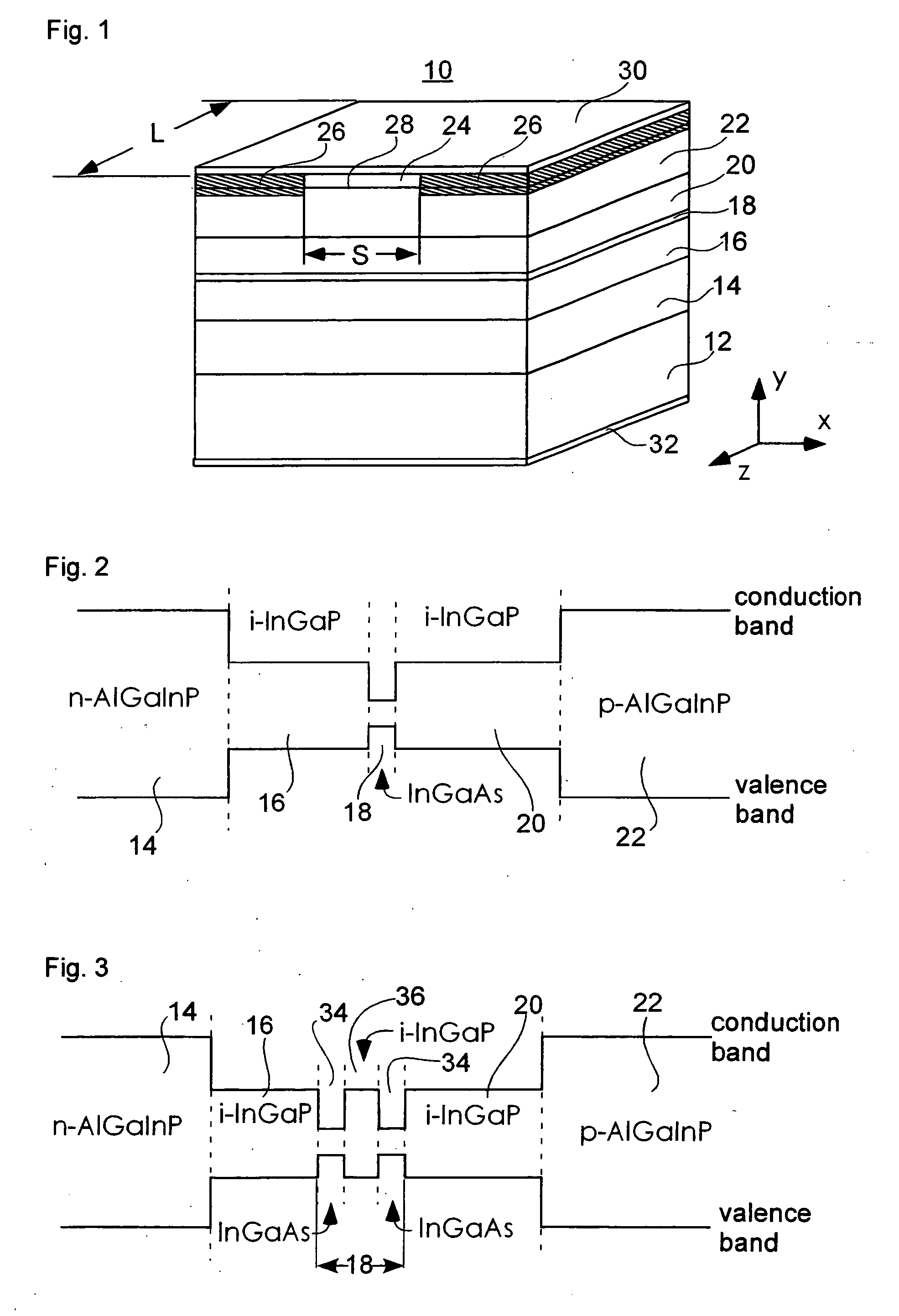
[0075]FIG. 1 is a perspective view of a semiconductor laser device according to one embodiment of the present invention. In the figures that follow, the same reference number indicates the same constituent element or equivalent.
[0076] In FIG. 1, a semiconductor laser 10 has emission wavelengths of a 940-nm band and is used as an pumping light source in solid-state laser of Yb-doped YAG laser, or others, or in Yb-doped fiber laser, Er-doped fiber amplifier, or other applications.
[0077] The semiconductor laser 10 includes the following layers each disposed in order on an n-GaAs substrate 12: an n-type cladding layer 14 as a first cladding layer, an n-side guide layer 16 as a first optical waveguide layer, an active layer 18 of a quantum well structure, a p-side guide layer 20 as a second optical waveguide layer, a p-type cladding layer 22 as a second cladding layer, and a contact layer 24 formed of p-GaAs.
[0078] At a connection section consist of the contact layer 24 and a layer wh...
second embodiment
[0150]FIG. 11 is a perspective view of a semiconductor laser according to one embodiment of the present invention.
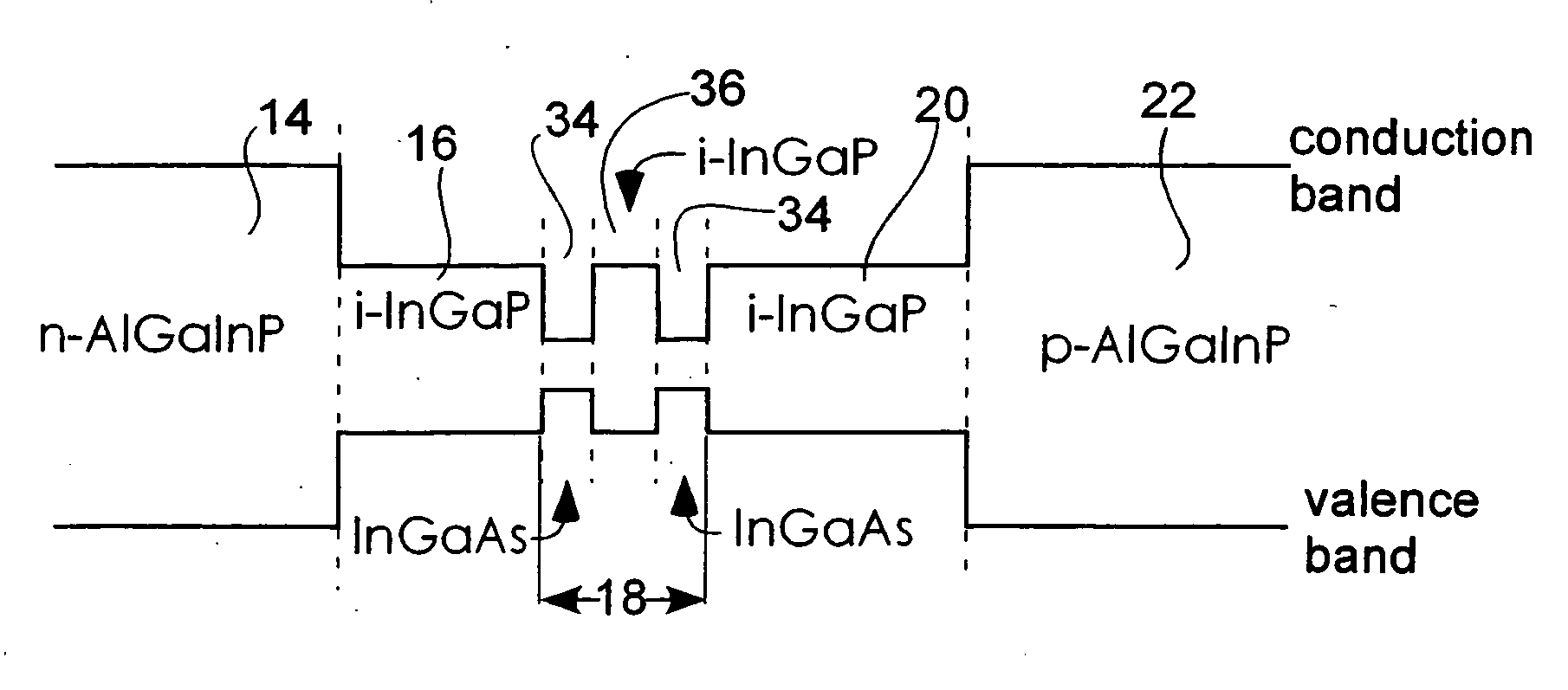
[0151] Semiconductor laser 54 in FIG. 11 differs from the semiconductor laser 10 of the first embodiment in that an n-side first barrier layer 56 is provided between an n-side guide layer 16 serving as a first barrier layer and an active layer 18, and in that a p-side first barrier layer 58 serving as another first barrier layer is provided between the active layer 18 and a p-side guide layer 20. Other structural aspects of the semiconductor laser 54 are the same as for the semiconductor laser 10.
[0152] The n-side first barrier layer 56 and the p-side first barrier layer 58 are both formed of i-GaAs0.88P0.12, an undoped semiconductor. Also, both the n-side first barrier layer 56 and the p-side first barrier layer 58 are 10 nm thick.
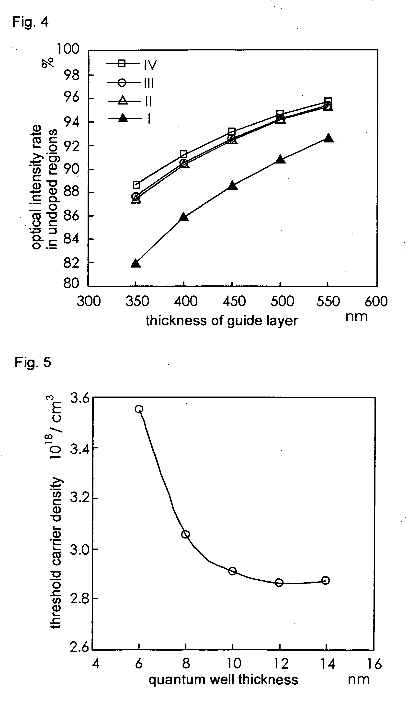
[0153]FIG. 12 is a graph showing optical intensity rates in undoped regions of the semiconductor laser according to one embodiment of the ...
third embodiment
[0190]FIG. 20 is a perspective view of a semiconductor laser according to one embodiment of the present invention.
[0191] Semiconductor laser 66 in FIG. 20 differs from the semiconductor laser 54 of the second embodiment in that in addition to an n-side first barrier layer 56, an n-side second barrier layer 68 is further provided as a second barrier layer between an n-side guide layer 16 and an active layer 18, and in that in addition to a p-side first barrier layer 58, a p-side second barrier layer 70 is further provided as a second barrier layer between the active layer 18 and a p-side guide layer 20.
[0192] In the semiconductor laser 66 of the present third embodiment, the n-side second barrier layer 68 is provided between the n-side guide layer 16 and the n-side first barrier layer56. Also, the p-side second barrier layer 70 is provided between the p-side first barrier layer 58 and the p-side guide layer 20. In the semiconductor laser 66, the n-side second barrier layer 68 and t...
PUM
 Abstract
Description
Claims
Application Information