Semiconductor laser device

a laser device and semiconductor technology, applied in the direction of lasers, semiconductor lasers, laser optical resonators, etc., can solve the problems of reducing luminous efficiency and increasing the threshold current of laser oscillation, and achieve high carrier concentration, small threshold current, and high luminous efficiency

Inactive Publication Date: 2007-05-15
MITSUBISHI ELECTRIC CORP
View PDF2 Cites 4 Cited by
  • Summary
  • Abstract
  • Description
  • Claims
  • Application Information

AI Technical Summary

Benefits of technology

[0008]The present invention has been devised to solve the above problems. It is, therefore, a first object of the present invention to provide a semiconductor laser device exhibiting a small threshold current and high luminous efficiency, in which electrons and holes are prevented from accumulating to a high carrier concentration in the semiconductor layer sandwiched by the two heterojunctions (double heterojunction).
[0010]Accordingly, a semiconductor laser device according to the present invention is configured such that: the bandgap energy of the fourth semiconductor layer is lower than those of the first and second semiconductor layers; and heterojunctions of the second kind are formed at the interfaces between the first and fourth semiconductor layers and between the second and fourth semiconductor layers. This arrangement prevents either minority carriers or majority carriers from accumulating in the fourth semiconductor layer, thereby reducing the probability of recombination between electrons and holes within the fourth semiconductor layer and hence reducing the recombination current.
[0011]Therefore, it is possible to prevent an increase in the threshold current and a reduction in the luminous efficiency due to the recombination current, providing a semiconductor laser device having high efficiency.

Problems solved by technology

When the carrier concentrations of the accumulated electrons and holes each have reached approximately 1×1018 cm−3 (hereinafter 1E18 cm−3), the electrons and holes combine within the diffraction grating layer and, as a result, an reactive current which does not contribute to the laser oscillation flows, causing the problem of increased threshold current of the laser oscillation and reduced luminous efficiency.

Method used


Image

  • Semiconductor laser device
  • Semiconductor laser device
  • Semiconductor laser device

Examples


first embodiment

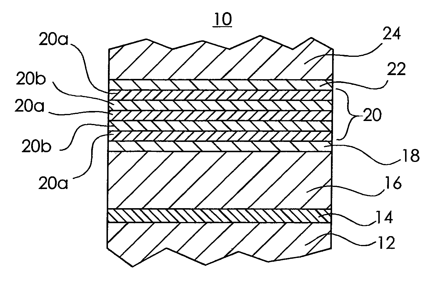
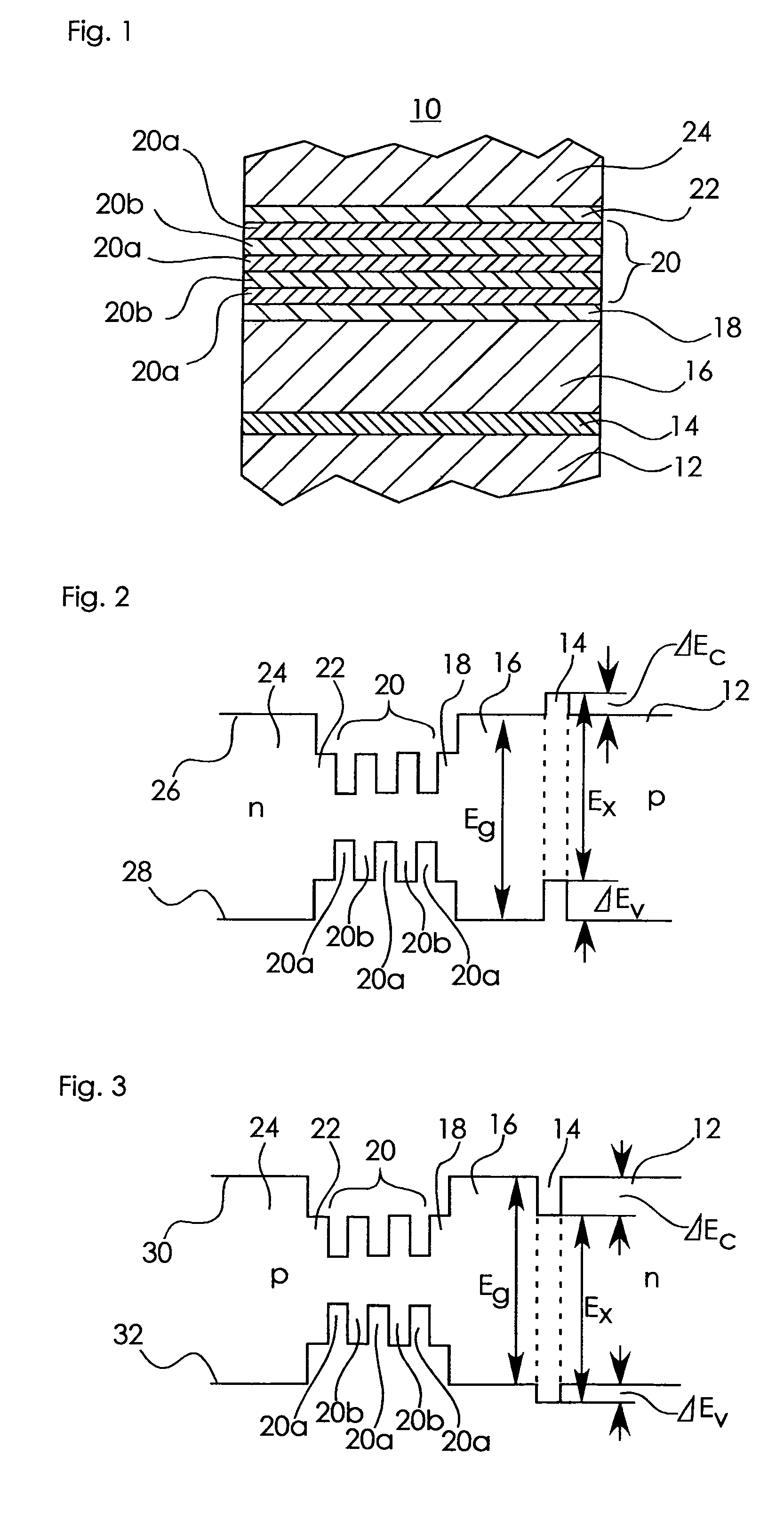
[0026]FIG. 1 is a cross-sectional view of a portion of a semiconductor laser device according to an embodiment of the present invention, the portion including an active layer and its neighborhood and having an optical waveguide laminated structure. It should be noted that in the following figures, like numerals will be used to denote like components.

[0027]FIG. 2 is a diagram showing the energy bands of the optical waveguide laminated structure shown in FIG. 1.

[0028]Referring to FIG. 1, a double heterojunction layer 14 is disposed on a first first-cladding layer 12, and a second first-cladding layer 16 is disposed on the double heterojunction layer 14. The first first-cladding layer 12 is made up of a p-type InP layer and acts as a first semiconductor layer (p-type and n-type are hereinafter abbreviated as “p-” and “n-”, respectively); the double heterojunction layer 14 is made of p-AlGaInAs and acts as a fourth semiconductor layer; and the second first-cladding layer 16 is made up o...

second embodiment

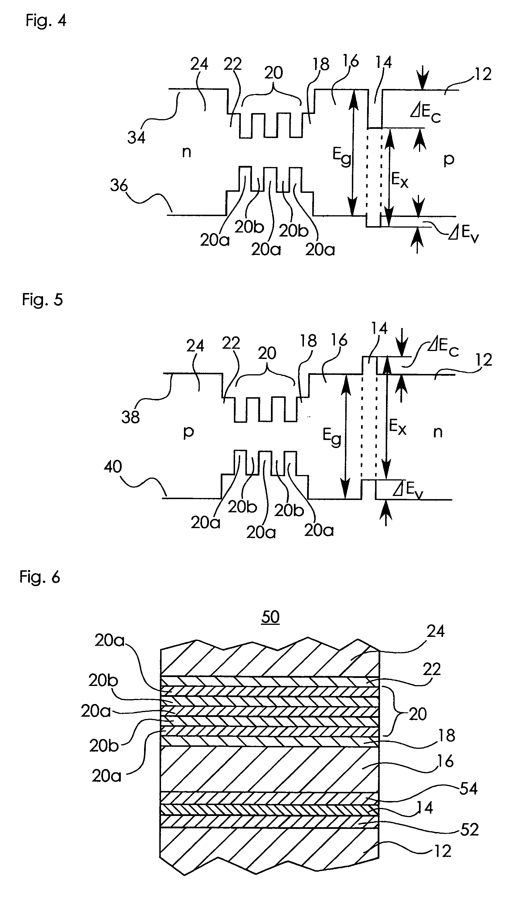
[0070]FIG. 6 is a cross-sectional view of a portion of a semiconductor laser device according to an embodiment of the present invention, the portion including an active layer and its neighborhood and having an optical waveguide laminated structure. FIG. 7 is a diagram showing the energy bands of the optical waveguide laminated structure shown in FIG. 6.

[0071]The basic configuration of the optical waveguide laminated structure 50 of the present embodiment is the same as that of the optical waveguide laminated structure 10 of the second variation (of the first embodiment). However, the optical waveguide laminated structure 50 is different from the optical waveguide laminated structure 10 of the second variation (of the first embodiment) in that the optical waveguide laminated structure 50 includes band discontinuity alleviating layers both between the first first-cladding layer 12 and the double heterojunction layer 14 and between the double heterojunction layer 14 and the second firs...

third embodiment

[0087]FIG. 9 is a cross-sectional perspective view of a portion of a semiconductor laser according to an embodiment of the present invention. FIG. 10 is a cross-sectional view of the semiconductor laser shown in FIG. 9 taken along line X—X.

[0088]Specifically, FIG. 9 shows a cross section of a distributed feedback semiconductor laser (hereinafter referred to as a DFB laser) 70 taken along a line in the optical waveguide direction (the x-axis direction); the semiconductor laser is symmetrical about this line. FIG. 10 shows a cross section of the DFB laser 70 taken along line X—X in the y-axis direction.

[0089]The DFB laser 70 is characterized in that its oscillation wavelength depends on the period of the diffraction grating and it can generate single-mode oscillation. This laser is also used for communications.

[0090]Referring to FIGS. 9 and 10, a first first-cladding layer 12 made up of a p-InP layer is disposed on a p-InP substrate 72 (the semiconductor substrate), and a double heter...


PUM


Abstract

A semiconductor laser device according to the present invention comprises an optical waveguide laminated structure having: a first first-cladding layer made up of a p-InP layer; a double heterojunction layer of p-AlGaInAs; a second first-cladding layer made up of a p-InP layer; a first light confining layer of p-InGaAsP; an active layer of InGaAsP having a quantum well structure; a second light confining layer of n-InGaAsP; and a second-cladding layer made up of an n-InP layer, and heterojunctions of the second kind are formed at the interfaces between the first first-cladding layer and the double heterojunction layer and between the double heterojunction layer and the second first-cladding layer.

Description

BACKGROUND OF THE INVENTION[0001]1. Field of the Invention[0002]The present invention relates to a semiconductor laser device, and more particularly to a semiconductor laser device used as a light source for optical communications and optical disk devices.[0003]2. Description of the Related Art[0004]High-capacity, recordable and portable optical disk systems are growing rapidly in popularity and use as external storage for personal computers, etc. Semiconductor laser devices having high optical output efficiency and good optical and temperature characteristics must be developed to satisfy the requirements of small or portable optical disk systems. On the other hand, with the spread of public networks using optical fibers, there is an increasing need to transmit a large amount of information at low cost. Increasing the information transmission rate so as to meet such a need requires a semiconductor laser device having high optical output efficiency.[0005]A known example of a conventi...

Claims


Application Information

Patent Timeline
Patent Type & Authority Patents(United States)
IPC IPC(8): H01S5/00H01S5/20H01S5/12H01S5/323H01S5/22H01S5/223H01S5/227H01S5/30H01S5/32H01S5/343
CPCB82Y20/00H01S5/2231H01S5/227H01S5/34313H01S5/12H01S5/2206H01S5/2214H01S5/2222H01S5/305H01S5/321H01S5/3211H01S5/3213H01S5/34353H01S5/34366H01S5/34373
Inventor TAKAGI, KAZUHISA
Owner MITSUBISHI ELECTRIC CORP
Why Eureka
Try Eureka