Semiconductor laser device and method of manufacturing the same

A technology of laser components and manufacturing methods, which is applied in the direction of semiconductor lasers, laser components, structures of optical waveguide semiconductors, etc. Characteristics and high-speed response characteristics, small threshold current, and good reliability

Inactive Publication Date: 2005-06-01
PANASONIC CORP
View PDF4 Cites 0 Cited by
  • Summary
  • Abstract
  • Description
  • Claims
  • Application Information

AI Technical Summary

Problems solved by technology

However, in the ridge-shaped semiconductor laser element described in the above-mentioned Japanese Patent Laid-Open No. 2003-46197, since the refractive index of the practical dielectric layer used for the barrier layer is small (minimum about 2), if the horizontal aperture angle (Δn: The actual difference in refractive index in the back of the ridge) necessitates designing the film thickness of the cladding layer under the barrier layer to be thick, so the reactive current increases and the threshold current also increases, so the temperature characteristics deteriorate. The problem
In addition, in order to form a current and light confinement structure, a dielectric layer with a lower thermal conductivity than a semiconductor layer is used, so there is a problem that the temperature characteristics of the device are further deteriorated.

Method used


Image

  • Semiconductor laser device and method of manufacturing the same
  • Semiconductor laser device and method of manufacturing the same
  • Semiconductor laser device and method of manufacturing the same

Examples


Embodiment Construction

[0054] Next, a semiconductor laser device according to an embodiment of the present invention will be described with reference to the drawings. In addition, although the structure and effect of the present invention have been described in more detail, the present invention is not limited to the following embodiments, and it is of course possible to add modifications within the scope of the purpose described above and below, all of which include Within the technical scope of the present invention.

[0055] (Embodiment 1)

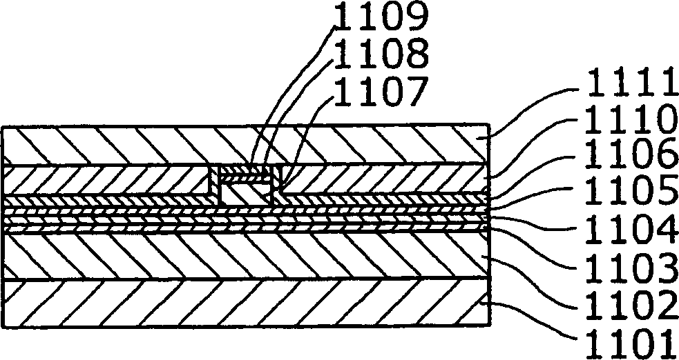
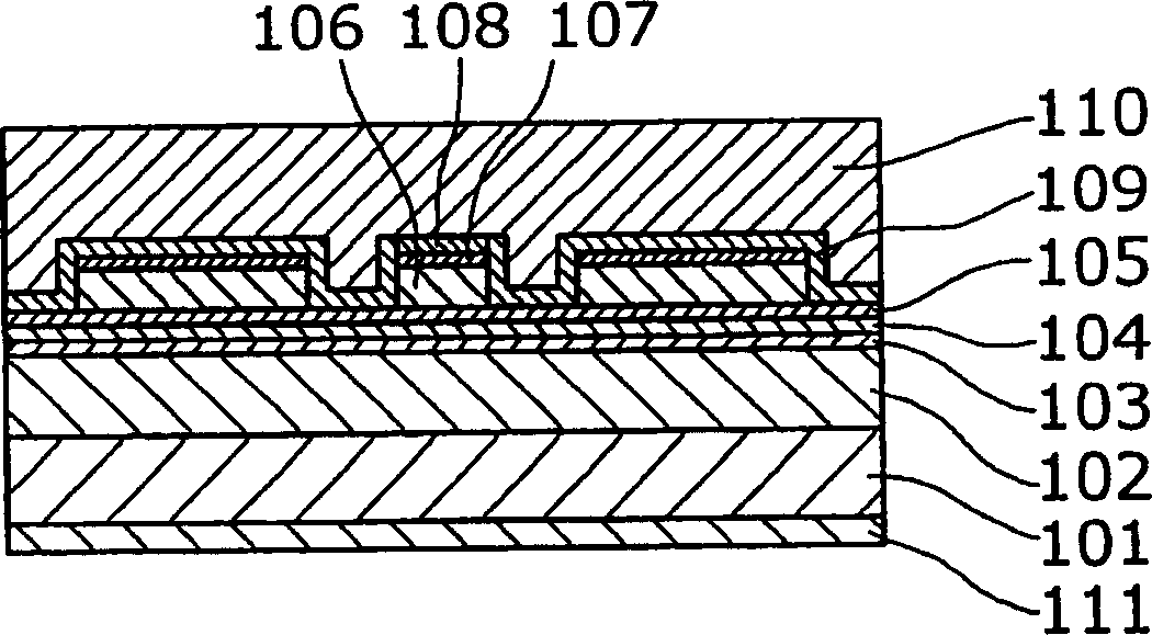
[0056] image 3 It is a cross-sectional view showing the structure of the semiconductor laser element of the first embodiment.

[0057] The semiconductor laser element of the present embodiment is a ridge-shaped semiconductor laser element, and in this semiconductor laser element, the n-type GaAs substrate 101 is sequentially stacked with 1×1018 cm -3 The n-type AlGaInP cladding layer 102 with a film thickness of 2 μm and the non-doped quantum well active ...


PUM

PropertyMeasurementUnit
thicknessaaaaaaaaaa
thicknessaaaaaaaaaa
thicknessaaaaaaaaaa

Abstract

The purpose of the present invention is to provide a semiconductor laser element with a small threshold current and easy fabrication, good temperature characteristics and high-speed response characteristics, which has an n-type GaAs substrate (101), an n-type GaAs substrate (101) The n-type AlGaInP cladding layer (102), the non-doped quantum well active layer (103), the p-type AlGaInP first cladding layer (104), the p-type GaInP corrosion stop layer (105), and the p-type AlGaInP second 2 cladding layer (106), p-type GaInP cladding layer (107), p-type GaAs contact layer (108) and n-type AlInP barrier layer (109), with ridges and protrusions on both sides of the ridges, p-type GaAs The contact layer (108) is formed only on top of the ridges.

Description

technical field [0001] The present invention relates to a semiconductor laser element, and more particularly to a semiconductor laser element used as a power source for an optical disk system, information processing, or optical communication. Background technique [0002] The semiconductor laser elements used in light sources such as optical disk systems are mainly ridge elements, and not only high output corresponding to fast writing is required, but also high-speed response (improved response speed to the light output rise characteristic of injection current). In order to realize high-speed responsiveness, it is necessary to reduce the resistance or capacitance of the laser element. [0003] In order to reduce the resistance, it is effective to enlarge the opening area of ​​the contact layer in the current injection region. In the conventional ridge semiconductor laser element, the verticality of the ridge is improved and the ridge is enlarged by using, for example, anisot...

Claims


Application Information

Patent Timeline
Patent Type & Authority Applications(China)
IPC IPC(8): H01S5/30H01S5/00H01S5/042H01S5/22H01S5/323
CPCH01S5/02476H01S5/22H01S5/222H01S5/32325H01S5/04254H01S5/30
Inventor 牧田幸治吉川兼司鹿岛孝之足立秀人
Owner PANASONIC CORP
Why Eureka
Try Eureka