Method and structure to reduce risk of gold embrittlement in solder joints

a technology of solder joints and gold embrittlement, applied in the direction of welding/cutting media/materials, manufacturing tools, solventing apparatus, etc., can solve the problems of inability to reduce the size of electrical devices, the solder joints may be exposed to temperature extremes, etc., and achieve the effect of reducing gold embrittlemen

Active Publication Date: 2006-02-28
TEXAS INSTR INC
View PDF6 Cites 5 Cited by
  • Summary
  • Abstract
  • Description
  • Claims
  • Application Information

AI Technical Summary

Problems solved by technology

After reflow, solder joints may be exposed to temperature extremes during use, testing, and possibly storage.
While prior attempts to reduce the creation of AuSn4 reduce the thickness of gold layer 222, this may not be practical with decreasing size of electrical devices.

Method used


Image

  • Method and structure to reduce risk of gold embrittlement in solder joints
  • Method and structure to reduce risk of gold embrittlement in solder joints
  • Method and structure to reduce risk of gold embrittlement in solder joints

Examples


Embodiment Construction

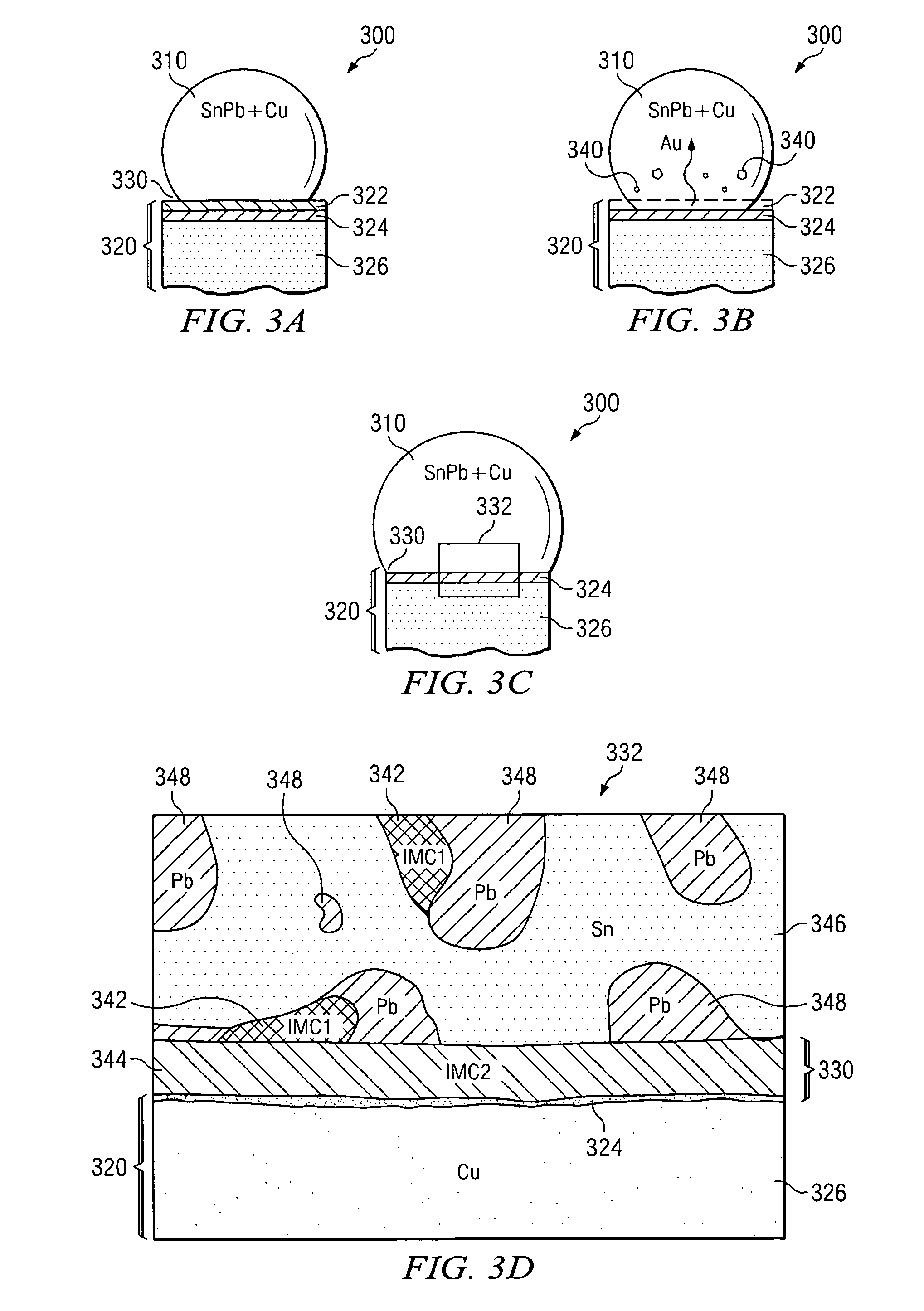
[0019]At least some embodiments of the invention involve adding copper to a non-copper bearing solder. The presence of copper within a solder may reduce the embrittlement of solder interconnects using gold-nickel pads. The various embodiments of the invention were developed in the context of adding copper to tin-lead solder to reduce embrittlement, and will therefore be described in that context; however, the description based on the developmental context should not be construed as a limitation on the types of solders to which copper may be added to reduce embrittlement.

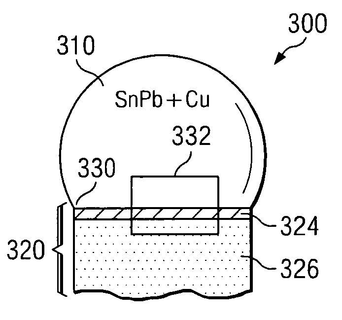
[0020]Referring now to FIG. 3A, a cross-sectional view is shown of a solder joint 300 comprising a solder interconnect 310 joined to a nickel-gold pad 320. The solder interconnect 310 may represent either a solder bump on a flip-chip die, a solder ball on a package substrate, or any other electronic interconnect. The pad 320 has a nickel-gold plating, which may comprise an outer gold layer 322 covering a nickel layer...


PUM

PropertyMeasurementUnit
temperaturesaaaaaaaaaa
electricalaaaaaaaaaa

Abstract

A method for reducing gold embrittlement in solder joints, and a copper-bearing solder according to the method, are disclosed. Embodiments of the invention comprise adding copper to non-copper based solder, such as tin-lead solder. The embodiments may further comprise using the copper-bearing solder as a solder interconnect on a gold-nickel pad.

Description

BACKGROUND OF THE INVENTION[0001]Integrated circuits are fabricated on the surface of a semiconductor wafer in layers and later singulated into individual dies. FIG. 1 shows a cross-sectional view of a semiconductor die assembly 100 including a flip-chip die 110. Die 110, which could be a microprocessor, mechanically and electrically couples to a package substrate 120 through an arrangement of solder bumps 152 on the active face 112 of the die. To attach the die 110 it is first “bumped,” or patterned with solder bumps 152. After bumping, the die 110 may be attached to an upper surface 134 of the package substrate 120 by melting the solder bumps 152, such as in an oven reflow process. An epoxy underfill material 130 may be introduced around the solder bumps 152 to improve solder joint reliability. Electrical communication through the package substrate 120 may be by way of conductive vertical columns, or substrate vias 124. Solder balls 180 attached to the bottom surface 136 of the pa...

Claims


Application Information

Patent Timeline
Patent Type & Authority Patents(United States)
IPC IPC(8): H01L23/48H01L23/52H01L29/40B23K35/00B23K35/26B23K35/30H01L23/31H01L23/485H01L23/498H05K3/24H05K3/34
CPCB23K35/26H01L24/13H01L23/49816H01L24/10H05K3/3463B23K35/007B23K35/262B23K35/268B23K35/302B23K2203/12H01L23/3128H01L2224/13099H01L2924/01015H01L2924/01029H01L2924/0103H01L2924/01049H01L2924/01078H01L2924/01079H01L2924/01082H01L2924/01322H01L2924/01327H01L2924/14H01L2924/19041H05K3/244H01L2924/01005H01L2924/01006H01L2924/01033H01L2924/01047H01L2924/014H01L2924/00H01L2224/13B23K2103/12A01K61/51
Inventor ZENG, KEJUN
Owner TEXAS INSTR INC
Why Eureka
Try Eureka