Method and apparatus to reduce bias temperature instability (BTI) effects

a temperature instability and bias technology, applied in pulse generators, instruments, pulse techniques, etc., can solve problems such as significant problems such as nbti caused vt shift in pfets, performance degradation, voltage sensitivity, etc., to reduce the effect of nbti caused vt shi

Inactive Publication Date: 2006-03-07
INT BUSINESS MASCH CORP
View PDF5 Cites 29 Cited by
  • Summary
  • Abstract
  • Description
  • Claims
  • Application Information

AI Technical Summary

Problems solved by technology

As a result of the shrinking sizes of the FETs and the reduction in VTs, Negative Bias Temperature Instability (NBTI) caused VT shifts in PFETs are becoming a significant problem that results in performance degradation, voltage sensitivity, and causing what might have been marginal but operative memory storage locations to become failing storage locations.
NBTI caused VT shift in PFETs is a significant problem in today's technology.
The increased temperature and supply voltage conditions applied during burn-in increases the rate of degradation due to NBTI caused VT shifts.
These patterns are needed but do not guarantee a 50% duty cycle on each bit line, word line, or storage element in the array.
Restarts on many electronic systems can be caused by manual intervention.

Method used


Image

  • Method and apparatus to reduce bias temperature instability (BTI) effects
  • Method and apparatus to reduce bias temperature instability (BTI) effects
  • Method and apparatus to reduce bias temperature instability (BTI) effects

Examples


Embodiment Construction

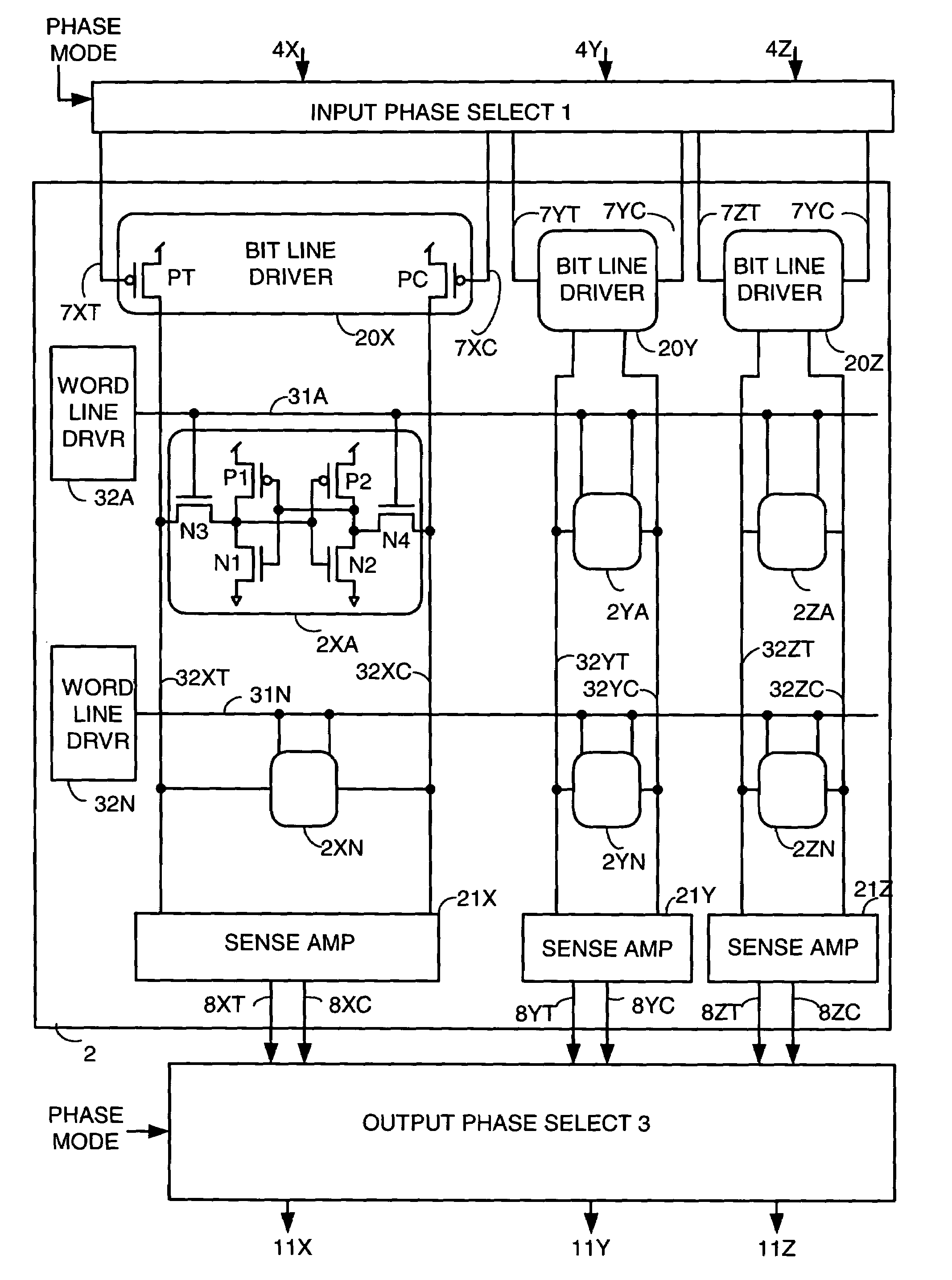
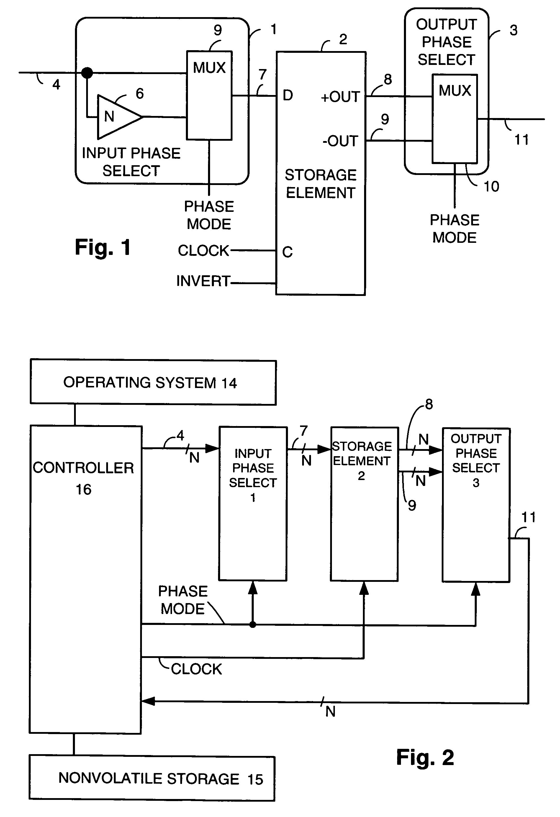
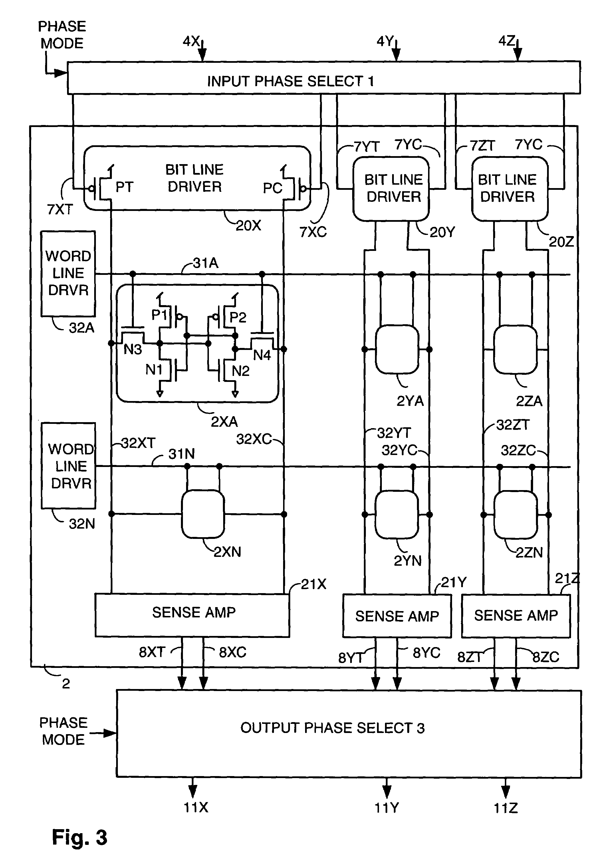
[0031]Having reference now to the figures, and having provided above a discussion of the art, the present invention will be described in detail.

[0032]The present invention generally provides methods and apparatus to reduce bias temperature instability (BTI) caused VT shift in FET circuits by making a duty cycle of many circuits, particularly storage elements, closer to being in a first voltage bias condition a first portion of the time an electronic system is used, and in a second voltage bias condition a second portion of the time the electronic system is used. The first voltage bias condition being an BTI voltage stress condition, the second voltage bias condition not being an BTI voltage stress condition. P-Channel FETS (PFETs) are particularly subject to negative bias temperature instability (NBTI) caused VT shifts in today's technology, however the present invention also contemplates positive bias temperature instability (PBTI) caused VT shifts in N-Channel FETs (NFETs). Becaus...


PUM


Abstract

Methods and apparatus are disclosed that allow an electronic system implemented with field effect transistors (FETs) to reduce threshold voltage shifts caused by bias temperature instability (BTI). BTI caused VT shifts accumulate when an FET is in a particular voltage stress condition. Many storage elements in an electronic system store the same data for virtually the life of the system, resulting in significant BTI caused VT shifts in FETs in the storage elements. An embodiment of the invention ensures that a particular storage element is in a first state for a first portion of time the electronic system operates, during which data is stored in a storage element in a first phase, and that the particular storage element is in a second state for a second portion of time the electronic system operates, during which data is stored in the storage element in a second phase.

Description

BACKGROUND OF THE INVENTION[0001]1. Field of the Invention[0002]The present invention generally relates to field effect transistor circuits. More specifically, the present invention relates to field effect transistors subject to bias temperature instability caused threshold voltage shifts.[0003]2. Description of the Related Art[0004]Modern electronic systems, for examples, computer processors, personal digital assistants (PDAs), digital cameras, currently rely on logic and storage circuits utilizing field effect transistors (FETs) fabricated on semiconductor chips. Complementary Metal Oxide Semiconductor (CMOS) circuits are widely used in such logic and storage circuitry because of the speed and relatively low power offered by CMOS circuits. CMOS circuits utilize P-channel field effect transistors (PFETs) and N-channel field effect transistors (NFETs).[0005]Recent advances in technology have reduced the physical sizes of the FETs. Voltage supplies have been reduced to save power as ...

Claims


Application Information

Patent Timeline
Patent Type & Authority Patents(United States)
IPC IPC(8): G11C7/04G11C7/10
CPCG11C7/1045G11C7/04
Inventor AIPPERSPACH, ANTHONY GUSHOVIS, WILLIAM PAULKUEPER, TERRANCE WAYNESHEETS, II, JOHN EDWARD
Owner INT BUSINESS MASCH CORP
Why Eureka
Try Eureka