
Method of optimizing and analyzing selected portions of a digital integrated circuit

Active Publication Date: 2006-03-07
GLOBALFOUNDRIES US INC
View PDF3 Cites 36 Cited by
  • Summary
  • Abstract
  • Description
  • Claims
  • Application Information

AI Technical Summary

Benefits of technology

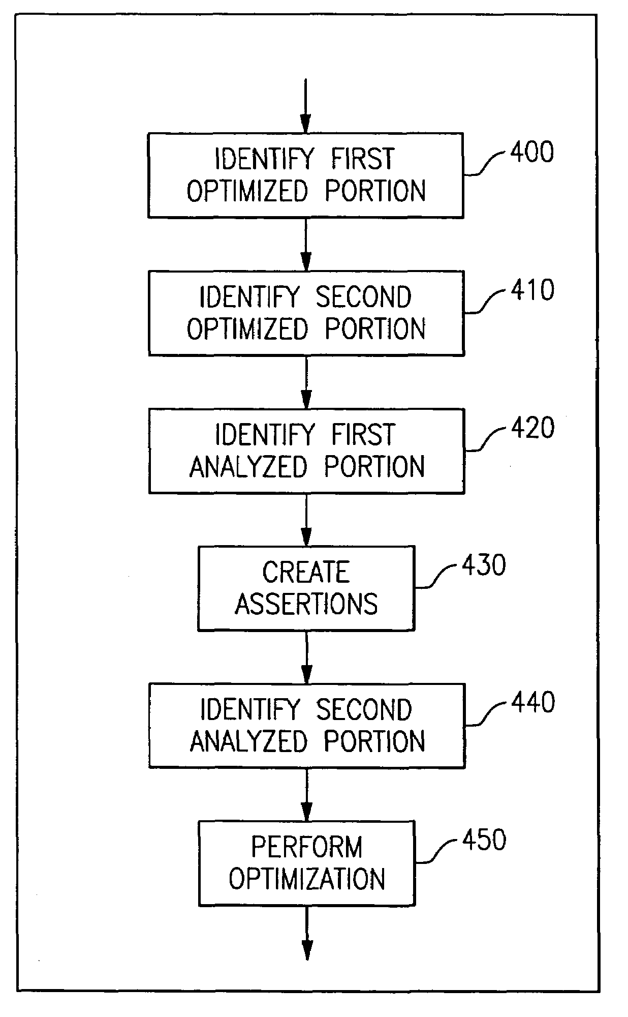
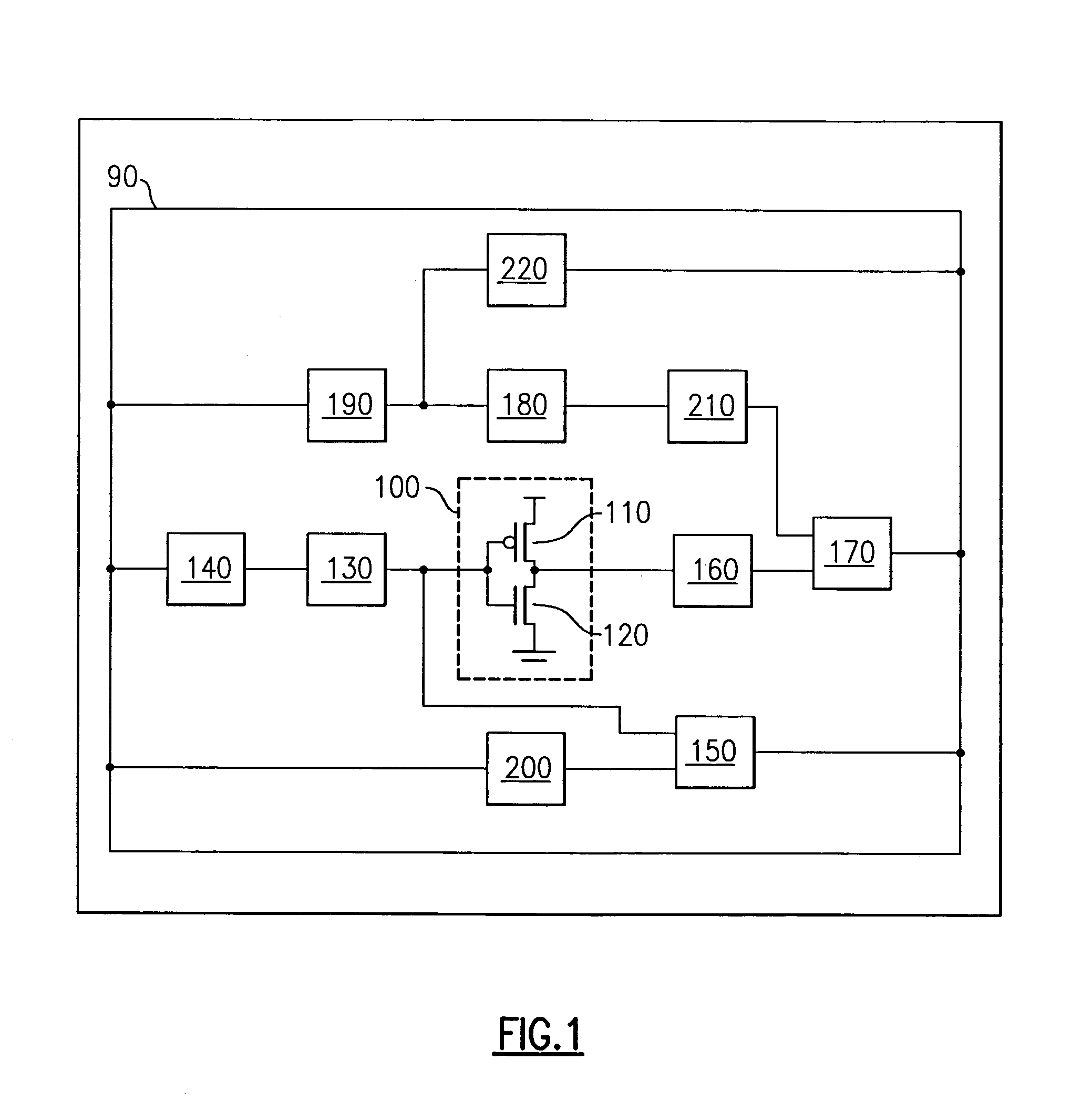
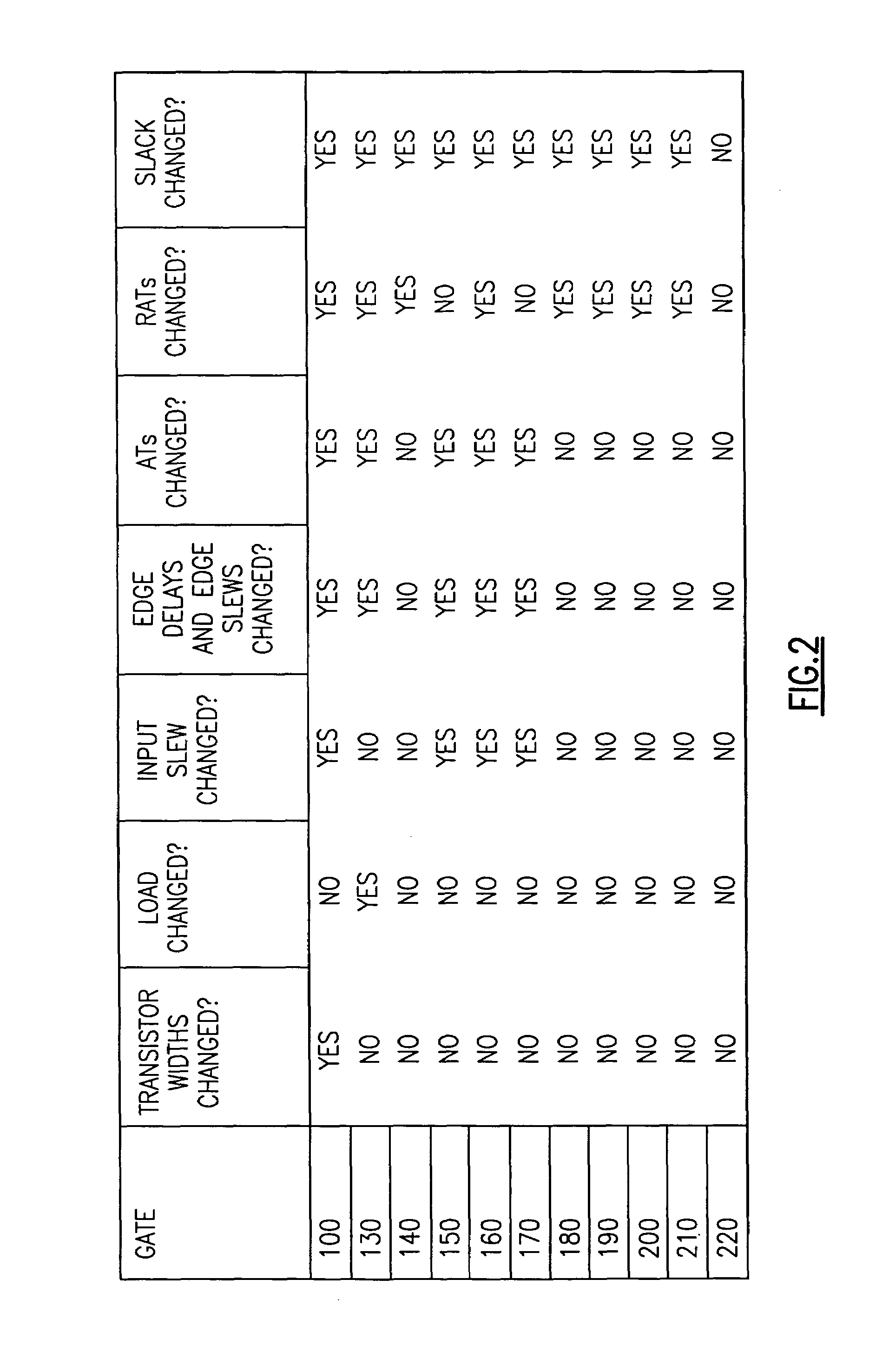
[0015]This invention relates to an improved method for achieving timing closure in the design of a digital integrated circuit or system by selecting portions of the circuit or system to be optimized and portions of the circuit or system in which the effects of such optimization are to be analyzed during the optimization process. A first optimized portion of the circuit or system will be identified containing those gates which will be modified, e.g., by having their transistor sizes changed. This first optimized portion will include timing critical portions of the circuit or system, i.e., those gates corresponding to nodes and edges in the timing graph which have a slack value below a first threshold, typically specified by the circuit designer, and which are therefore limiting the performance of the circuit or system. An optional second optimized portion of the circuit or system will include highly timing-noncritical portions of the circuit or system in which the slack is above a second threshold, because gates in these portions are likely to be able to be significantly reduced in size or power without limiting circuit or system performance, and hence the optimization may “steal” area or power from them, using it to speed up the critical portion of the circuit or system without violating overall area or power constraints. In addition to the portion of the circuit o

Problems solved by technology

Because of the dependence of edge delay and edge slew on load, changes to the sizes of transistors in a gate will also affect the edge delays and edge slews of input gates feeding the gate, and these will in turn affect the node slews, edge slews, edge delays, and ATs of all nodes and edges in the fanout cone of the input gates.
Many of the optimization techniques used to achieve timing closure have practical limits on the size of the circuit or system to which they can be applied, due to memory, runtime, or numerical noise, and are therefore typically applied to small partitions of a circuit or system.
Such partitioning can cause disruption to other steps in the design process.
In addition, any partition boundary constraints determined before optimization of the circuit or system partitions are unable to account for the effects of the subsequent optimization, and will therefore result in unequal effort being applied to different portions of critical paths cut by these partition boundaries, and thus in a sub-optimal result.

Method used


Image

  • Method of optimizing and analyzing selected portions of a digital integrated circuit
  • Method of optimizing and analyzing selected portions of a digital integrated circuit
  • Method of optimizing and analyzing selected portions of a digital integrated circuit

Examples


Embodiment Construction

[0025]The inventive method applies to the design of a digital integrated circuit or system which is to be optimized to operate at a specified clock period, to reduce the minimum clock period at which the circuit or system can operate, and optionally to reduce the portion of the circuit or system (e.g., the number of gates) which are in paths which limit the clock period at which the circuit or system will operate. It may equally apply to the design of a partition of a circuit or system.

[0026]The general goal of circuit or system optimization is to minimize some objective function subject to a set of constraints. The objective may include the clock period at which the circuit or system can operate, circuit or system area or power, or some combination of these and / or other objectives. Optimization constraints can include the clock period at which the circuit or system can operate, circuit or system area or power, slews, beta ratios of gates (the ratio between the “strength,” or effect...


PUM


Abstract

Disclosed is a method for achieving timing closure in the design of a digital integrated circuit or system by selecting portions of the circuit or system to be optimized and portions of the circuit or system in which the effects of such optimization are to be analyzed during the optimization process. Optimized portions will include gates whose design parameters are to be changed, a first analyzed portion includes gates whose delays and edge slews are to be recomputed, and a second analyzed portion includes gates whose ATs and RATs are to be recomputed during optimization. Constraints are imposed at selected boundaries between these portions to prevent unwanted propagation of timing information and to ensure the validity of timing values used during optimization. Through this selection, the size of the problem posed to the underlying optimization method will be reduced, allowing larger circuits or systems to be optimized and allowing optimization to be performed more quickly.

Description

RELATED APPLICATIONS[0001]D. J. Hathaway, C. Visweswariah, P. M. Williams, and J. Zhou, “Method of Achieving Timing Closure in Digital Integrated Circuits by Optimizing Individual Macros,” filed May 12, 2003 as U.S. Ser. No. 10 / 435,824 (0079).[0002]E. K. Cho, D. J. Hathaway, M. Hsu, L. K. Lange, G. A. Northrop, C. Visweswariah, C. Washburn, P. M. Williams, J. Zhou, “A Method for Tuning a Synthesized Random Logic Circuit Macros in a Continuous Design Space With Optimal Insertion of Multiple Threshold Voltage Devices,” filed May 10, 2004, as U.S. Ser. No. 10 / 842,589 (0206).FIELD OF THE INVENTION[0003]This invention relates to the design, and automation thereof, of high-performance digital integrated circuits. The invention is particularly directed to the problem of designing a digital integrated circuit or system, or portion thereof, which satisfies performance and other requirements by optimizing and analyzing a subset of the component gates or other elements that constitute the circ...

Claims


Application Information

Patent Timeline
IPC IPC(8): G06F17/50
CPCG06F17/505G06F30/327
Inventor HATHAWAY, DAVID J.LANGE, LAWRENCE KENNETHVISWESWARIAH, CHANDRAMOULIWILLIAMS, PATRICK M.
Owner GLOBALFOUNDRIES US INC
Learn More