
High-voltage integrated CMOS circuit

Inactive Publication Date: 2006-03-14
STMICROELECTRONICS SRL
View PDF5 Cites 2 Cited by
  • Summary
  • Abstract
  • Description
  • Claims
  • Application Information

AI Technical Summary

Benefits of technology

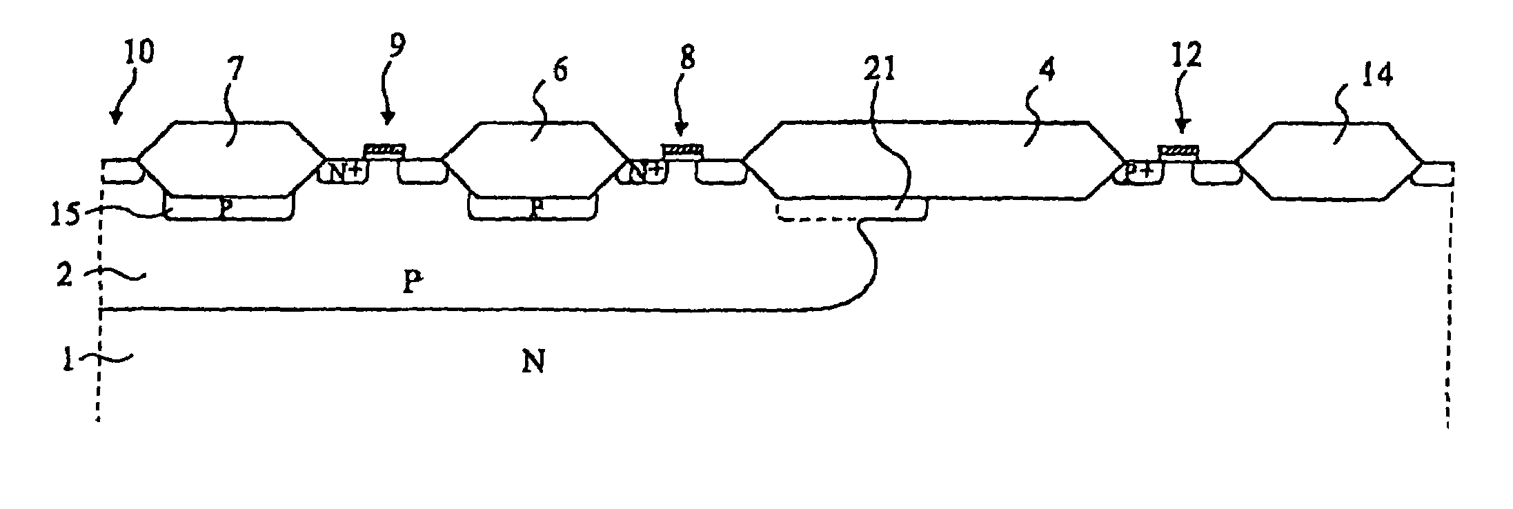
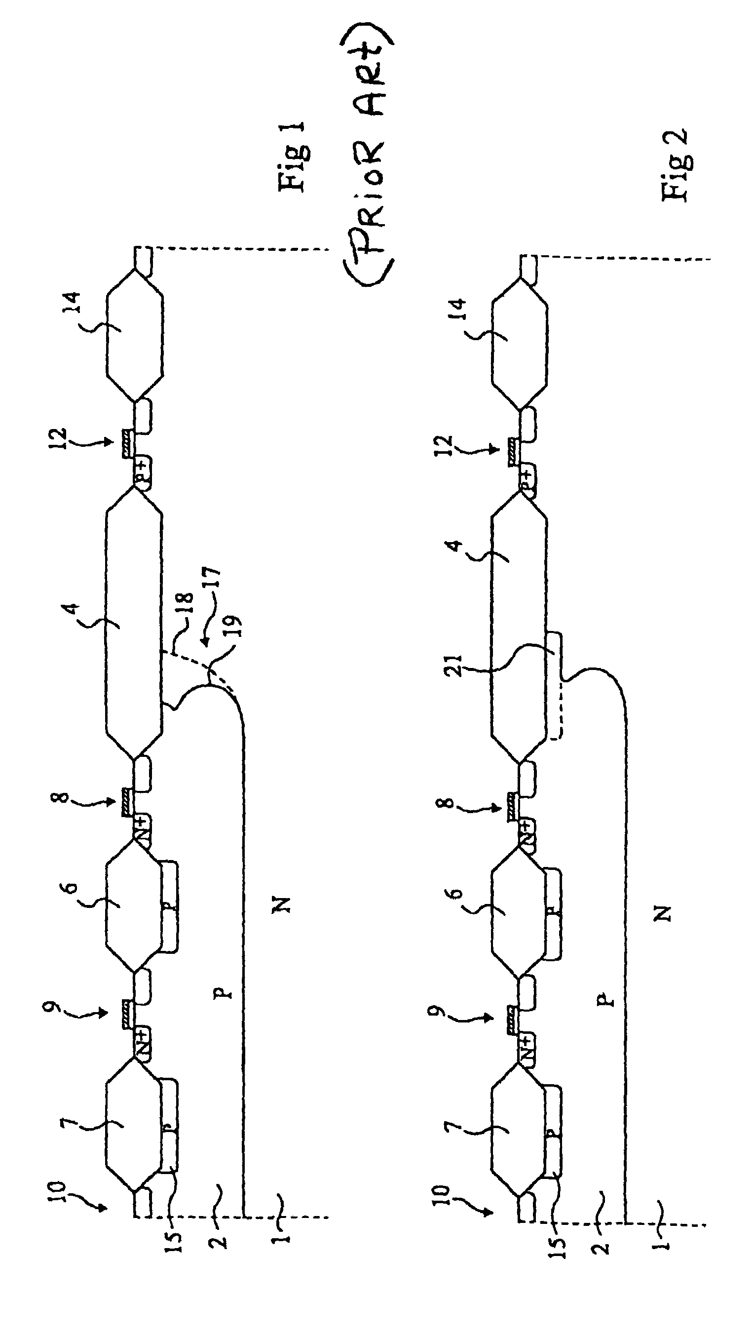
[0013]Thus, an object of the present invention is to provide a novel retrograde well periphery structure that improves the reverse breakdown voltage of this well. The present invention aims at achieving this object without increasing the manufacturing cost of a component and without increasing the number of technological steps necessary to its implementation.

Problems solved by technology

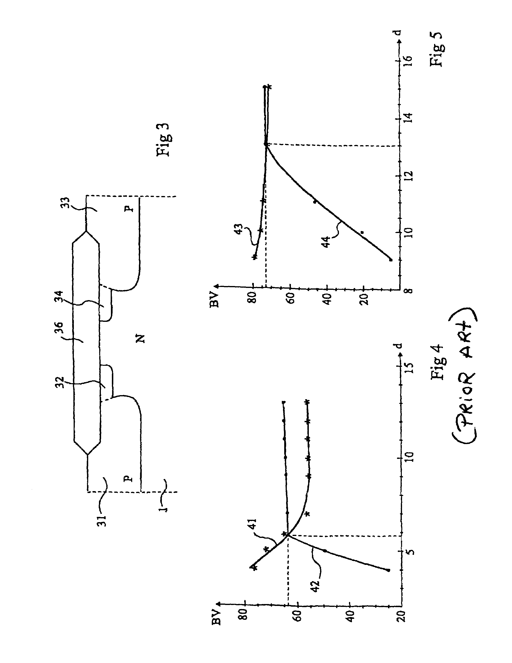
However, such retrograde-type wells appear in practice to have a smaller breakdown voltage in reverse biasing, that is, when well P is negatively charged with respect to substrate 1, than conventional wells in which the doping level progressively decreases from the upper surface to the lower area of the well.
This solution has a limited efficiency and does not, by itself sufficiently increase the breakdown voltage.
It can thus not be adopted when the manufacturing cost of a component is desired to be lowered.

Method used


Image

  • High-voltage integrated CMOS circuit
  • High-voltage integrated CMOS circuit
  • High-voltage integrated CMOS circuit

Examples


Embodiment Construction

[0024]Having thus described at least one illustrative embodiment of the invention, various alterations, modifications, and improvements will readily occur to those skilled in the art. Such alterations, modifications, and improvements are intended to be within and scope of the invention. Accordingly, the foregoing description is by way of example only and is not as limiting. The invention is limited only as defined in the following claims and the equivalents thereto.

[0025]FIG. 2 shows same elements as in FIG. 1 having the same reference characters. These elements will not be described again. The difference between the structures according to the present invention shown in FIG. 2 and the prior art structure shown in FIG. 1 is the structure of the area peripheral to the well. As previously, this periphery extends under a thick oxide inter-well area 4. Well 2 is a retrograde well formed in the same way as described in relation with FIG. 1. However, under a portion of insulating inter-we...


PUM


Abstract

The invention relates to an integrated CMOS circuit comprising, in a semiconductor substrate (1) with a first type of conductivity, a casing (2) of a second type of retrograde-doped conductivity, the end of said casing being covered by an inter-casing insulating region (4). The components contained in said casing are separated from each other by means of intra-casing insulating regions (6,7). The first insulating elements (15) of the second type of high-level doping conductivity extend under each intra-casing insulating region. A second region (21) of the second type of high-level doping conductivity partially extends under the inter-casing insulator beyond the periphery of each casing.

Description

BACKGROUND OF THE INVENTION[0001]1. Field of the Invention[0002]The present invention relates to the manufacturing of a CMOS-type integrated circuit.[0003]2. Discussion of the Related Art[0004]In a CMOS-type integrated circuit, various components are formed within properly doped wells. The substrate is of a first conductivity type, for example, an N-type epitaxial layer laid on an N+-type wafer, and wells having a conductivity type opposite to that of the substrate, for example P wells, will more specifically be considered herein in the case where they have a retrograde doping. A retrograde doping well is a well formed by a succession of at least one deep implantation at a high doping level and at least one shallower implantation at a lower concentration. Such structures have the advantage of reducing the necessary thermal processings and limiting the gain of vertical parasitic transistors.[0005]An example of such a structure is illustrated in FIG. 1. A lightly-doped N-type substrat...

Claims


Application Information

Patent Timeline
IPC IPC(8): H01L29/76H01L21/76H01L21/8238H01L27/08H01L27/092
CPCH01L27/092H01L21/8238
Inventor GERMANA, ROSALIA
Owner STMICROELECTRONICS SRL
Learn More