
Vertical power component

Inactive Publication Date: 2005-06-07
STMICROELECTRONICS SRL
View PDF13 Cites 0 Cited by
  • Summary
  • Abstract
  • Description
  • Claims
  • Application Information

AI Technical Summary

Benefits of technology

[0011]Thus, an object of the present invention is to provide a novel method of manufacturing power components intended for or optimize the thickness of the most lightly doped breakdown voltage layer.

Problems solved by technology

Under this threshold, they would be likely to break too easily in handling associated with the manufacturing process.
Otherwise, during this long thermal processing time, the implantations previously performed in the substrate would diffuse too deeply.
However, an excessive thickness of this area results in an increase of on-state losses of the power device.
No simple way of solving this problem is currently known.
Indeed, increasing, for example, the thickness of layer 4 has the consequence that the junction profile of this layer risks not fulfilling the desired electric conditions.
More generally, the same problem is raised with any power device to be surrounded with an isolating wall, the rear surface of which is of a doping type opposite to that of a breakdown voltage substrate, for example a power transistor or an IGBT transistor.

Method used


Image

  • Vertical power component
  • Vertical power component

Examples


Embodiment Construction

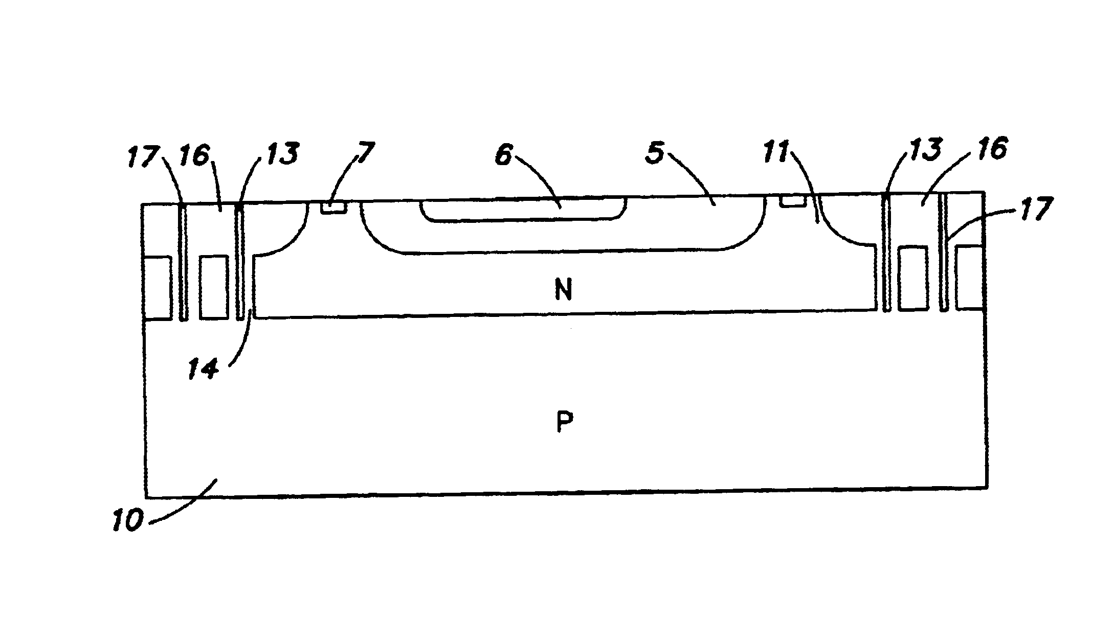
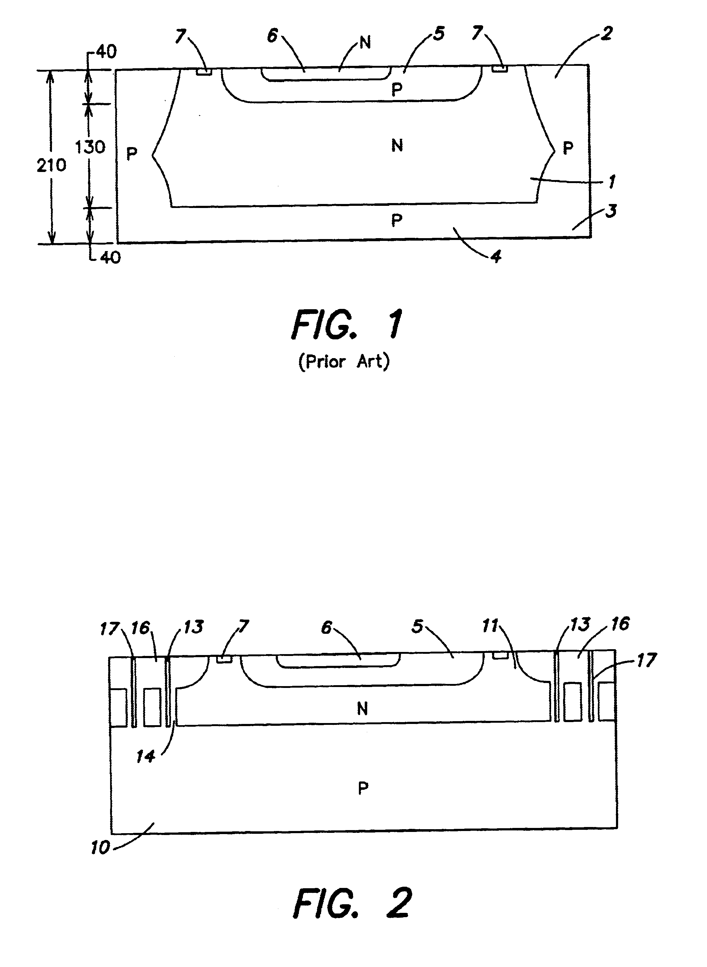
[0021]According to the present invention, to form a power component, on a relatively heavily-doped P-type substrate 10 is first formed by the epitaxy of a lightly-doped N-type layer 11 intended to form the breakdown voltage layer of a vertical power component, of which the P substrate forms the lower surface anode. Then, to form an isolating wall, the present invention provides forming a trench 13 substantially crossing the thickness of epitaxial layer 11 and surrounding the component, then diffusing a dopant 14 from this trench. For example, the trench will be filled with heavily-doped P-type polysilicon and a thermal diffusion step will be performed. The time required by the diffusion will be extremely short as compared to the time required by the steps of vertical deep diffusion of the isolating walls described in relation with FIG. 1.

[0022]According to an alternative of the present invention, the trench is replaced with openings sufficiently close to one another for diffused are...


PUM


Abstract

A vertical power component on a silicon wafer, including a lightly-doped epitaxial layer of a second conductivity type on the upper surface of a heavily-doped substrate of a first conductivity type, the epitaxial layer having a thickness adapted to withstanding the maximum voltage likely to be applied to the power component during its operation; and an isolating wall formed by etching a trench through the epitaxial layer and diffusing from this trench a dopant of the first conductivity type of high doping level.

Description

CROSS REFERENCE TO RELATED APPLICATIONS[0001]This application is a division of prior application Ser. No. 09 / 705,292, filed on Nov. 2, 2000 now U.S. Pat. No. 6,551,868, entitled Vertical Power Component Manufacturing Method, now allowed.BACKGROUND OF THE INVENTION[0002]1. Field of the Invention[0003]The present invention relates to power components of vertical type capable of withstanding high voltages.[0004]2. Discussion of the Related Art[0005]FIG. 1 is a very simplified cross-section view illustrating the general structure of a conventional power component. This component is formed in a large silicon wafer and is surrounded at its external periphery with an isolating wall of a conductivity type opposite to that of the substrate. This isolating wall is intended to separate the component from other components on the same chip, or for creating an electrically inactive protection area at the border of a chip, where a cutting is performed with respect to a neighboring chip. More speci...

Claims


Application Information

Patent Timeline
IPC IPC(8): H01L29/06H01L21/70H01L21/761H01L21/763H01L29/02H01L29/74H01L21/225H01L21/331H01L21/332H01L21/76H01L29/739H01L29/78
CPCH01L21/761H01L21/763H01L29/74H01L29/66393H01L29/0619H01L21/2257H01L29/66333
Inventor AURIEL, GERARDCORNIBERT, LAURENT
Owner STMICROELECTRONICS SRL
Learn More