
Microelectronic assemblies incorporating inductors

a technology of inductors and microelectronic assemblies, which is applied in the direction of inductances, program/content distribution protection, instruments, etc., can solve the problems of increasing the size and cost of chips, and it is difficult to provide substantial inductance in chips fabricated using conventional chip-making techniques, so as to reduce inductive coupling

Inactive Publication Date: 2006-03-14
TESSERA INC
View PDF88 Cites 49 Cited by
  • Summary
  • Abstract
  • Description
  • Claims
  • Application Information

AI Technical Summary

Benefits of technology

This approach enables the creation of high-inductance, compact inductors that can be integrated within microelectronic packages, enhancing thermal management and signal propagation while maintaining a compact form factor and reducing size and cost.

Problems solved by technology

While some passive components can be incorporated in the semiconductor chip itself, this adds to the size and cost of the chip.
Moreover, it is difficult to provide substantial inductance in chips fabricated using conventional chip-making techniques.

Method used


Image

  • Microelectronic assemblies incorporating inductors
  • Microelectronic assemblies incorporating inductors
  • Microelectronic assemblies incorporating inductors

Examples


Embodiment Construction

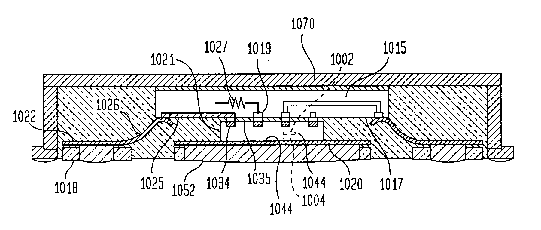
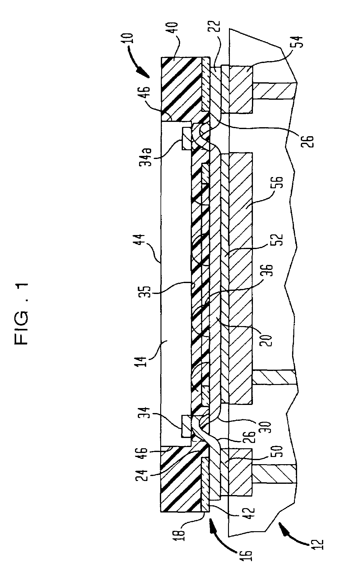
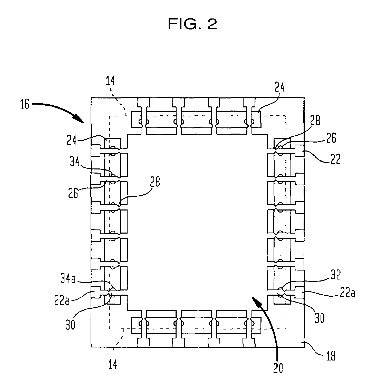
[0048]As further discussed below, certain aspects of the invention provide inductors formed as elements of chip assemblies such as packaged chips or modules. Accordingly, a few non-limiting examples of such chip assemblies are discussed herein. FIG. 1 shows a diagrammatic sectional view of a chip assembly. The assembly includes a packaged chip 10 mounted to a circuit board 12. The packaged chip 10 includes a chip or “die”14 and a chip carrier 16. FIG. 2 shows a diagrammatic plan view of the die 14 and chip carrier 16 of FIG. 1 at an intermediate stage during fabrication of the packaged chip. The chip carrier 16 includes a dielectric layer 18 which desirably is a thin, flexible layer of a polymeric dielectric as, for example, polyimide or BT resin. The chip carrier has a large metallic thermal conductor 20 in a central region and a plurality of terminals 22 in a peripheral region surrounding the central region. The dielectric also has apertures or bond windows 24 extending through th...


PUM


Abstract

Inductors are provided in chip assemblies such as in packaged semiconductor chips. The inductors may be incorporated in a chip carrier which forms part of the package, and may include, for example, spiral or serpentine inductors formed from traces on the chip carrier. The chip carrier may include a flap bearing the inductive element, and this flap may be bent to tilt the inductive element out of the plane of the chip carrier to reduce electromagnetic interaction between the inductive element and surrounding electrical components. Other inductors include solenoids formed in part by leads on the chip carrier as, for example, by displacing leads out of the plane of the chip carrier to form loops in vertically-extensive planes transverse to the plane of the chip carrier. Additional features provide trimming of the inductor to a desired inductance value during by breaking or connecting leads during assembly.

Description

CROSS-REFERENCE TO RELATED APPLICATIONS[0001]This application is a continuation-in-part of International Patent Application PCT / US02 / 27509 designating the U.S., filed Aug. 28, 2002, which in turn is a continuation-in-part of U.S. patent application Ser. No. 10 / 210,160, filed Aug. 1, 2002 now U.S. Pat. No. 6,856,007, which in turn claims benefit of U.S. Provisional Patent Application Ser. No. 60 / 315,408 filed Aug. 28, 2001. This application is also a continuation-in-part of said U.S. patent application Ser. No. 10 / 210,160, filed Aug. 1, 2002 now U.S. Pat. No. 6,856,007, which in turn claims benefit of U.S. Provisional Patent Application Ser. No. 60 / 315,408 filed Aug. 28, 2001. The disclosures of the above-mentioned applications are hereby incorporated by reference herein.BACKGROUND OF THE INVENTION[0002]The present application relates to microelectronic assemblies including inductors, and to components and methods useful in making such assemblies.[0003]Semiconductor chips or dies com...

Claims


Application Information

Patent Timeline
Patent Type & Authority Patents(United States)
IPC IPC(8): H01L23/48G06F21/00H01L23/24H01L23/31H01L23/367H01L23/433H01L23/498H01L23/552H01L23/64H01L25/065H03H9/05H03H9/10
CPCH01F17/0033H01L23/24H01L23/3107H01L23/3114H01L23/36H01L23/3675H01L23/4334H01L23/49531H01L23/49575H01L23/49822H01L23/49838H01L23/49861H01L23/5387H01L23/552H01L23/645H01L24/49H01L25/0652H01L25/0657H01L25/16H01L2223/6611H01L2224/16145H01L2224/48091H01L2224/4824H01L2224/4911H01L2224/73253H01L2224/73257H01L2224/73265H01L2225/0651H01L2225/06513H01L2225/06517H01L2225/0652H01L2225/06527H01L2225/06541H01L2225/06551H01L2225/06572H01L2225/06579H01L2225/06582H01L2924/01005H01L2924/01006H01L2924/01007H01L2924/01013H01L2924/01014H01L2924/01027H01L2924/01028H01L2924/01029H01L2924/01031H01L2924/01047H01L2924/0105H01L2924/01061H01L2924/01078H01L2924/01079H01L2924/01082H01L2924/01322H01L2924/01327H01L2924/15311H01L2924/1532H01L2924/15331H01L2924/16152H01L2924/19041H01L2924/19042H01L2924/19043H01L2924/19103H01L2924/19107H01L2924/3011H01L2924/3025H01L24/48H01L2924/01023H01L2924/01033H01L2924/01087H01L2924/014H01L2924/10253H01L2924/30107H01L2924/00014H01L2924/00H01L2924/15787H01L2224/451H01L2224/45014H01L2924/12042H01L2224/85207H01L24/45H01L2224/16235H01L2224/05571H01L2224/05573H01L2224/05569H01L2224/32245G06F21/10H01L24/50H03H9/0542H03H9/0547H03H9/1064G06F2221/2129H01L2224/05599H01L2224/12105H01L2224/32145H01L2224/45099H01L2224/48145H01L2224/48225H01L2224/48227H01L2224/73204H01L2224/73207H01L2224/85399H01L2924/01075H01L2924/19011H01L2924/19104H01L2924/19105H01L2924/30105H03H2009/0019H01L2225/06568H01L24/86H01L24/17H01L2224/17519H01L2224/08225H01L2224/32225H01L2224/16265H01L24/73H01L24/32H01L24/05H01L24/16H01L2224/131H01L2224/45015H01L2924/207H01L2924/00012H01L2224/16225Y04S40/20
Inventor WARNER, MICHAELHABA, BELGACEMBEROZ, MASUD
Owner TESSERA INC
Learn More