

Method for producing a capacitor-embedded circuit board
- Summary
- Abstract
- Description
- Claims
- Application Information
AI Technical Summary
Benefits of technology
Problems solved by technology
Method used
Image

Examples
embodiment 1
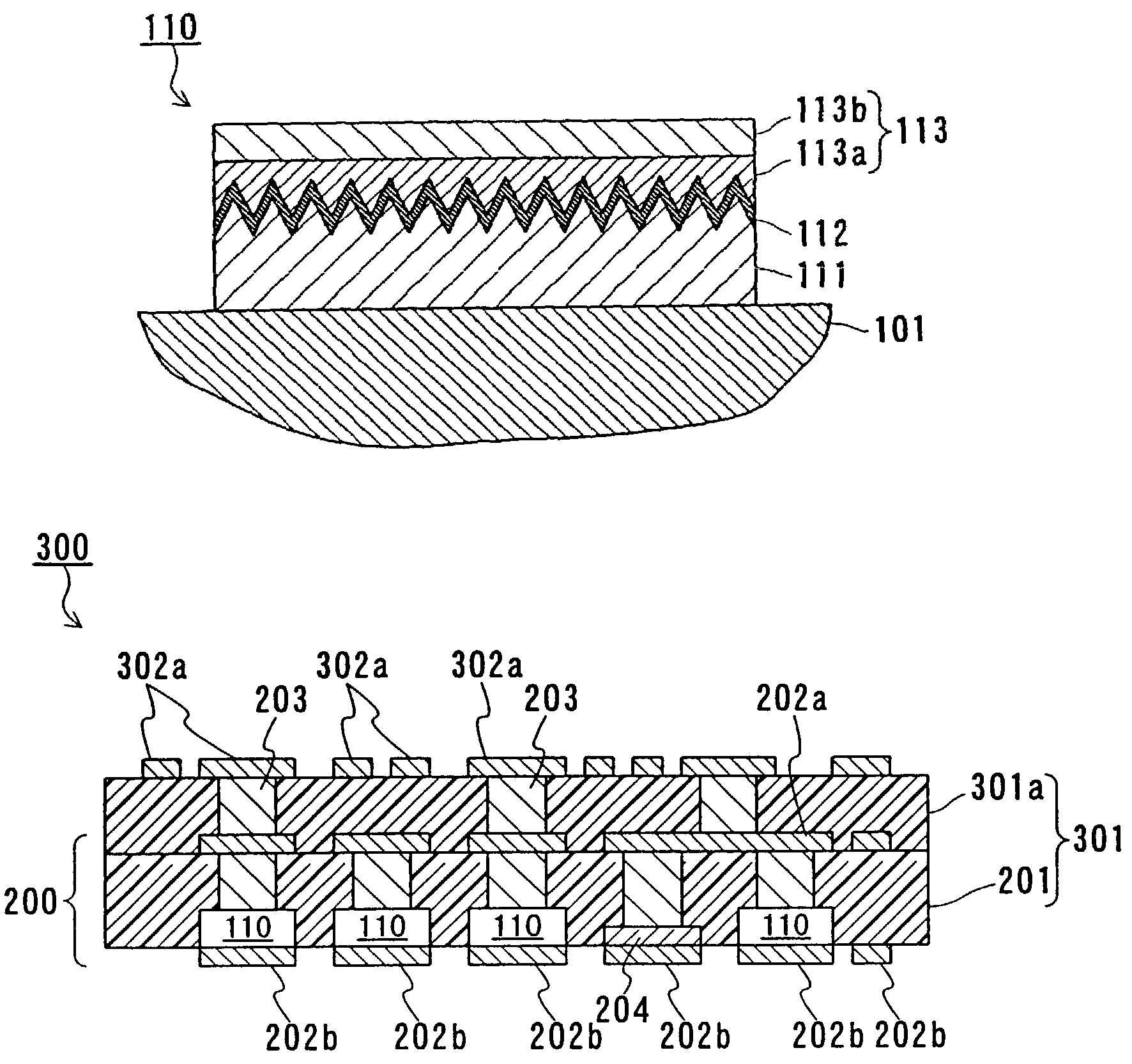
[0077]In Embodiment 1, an example of a capacitor-mounted metal foil of the present invention will be described.
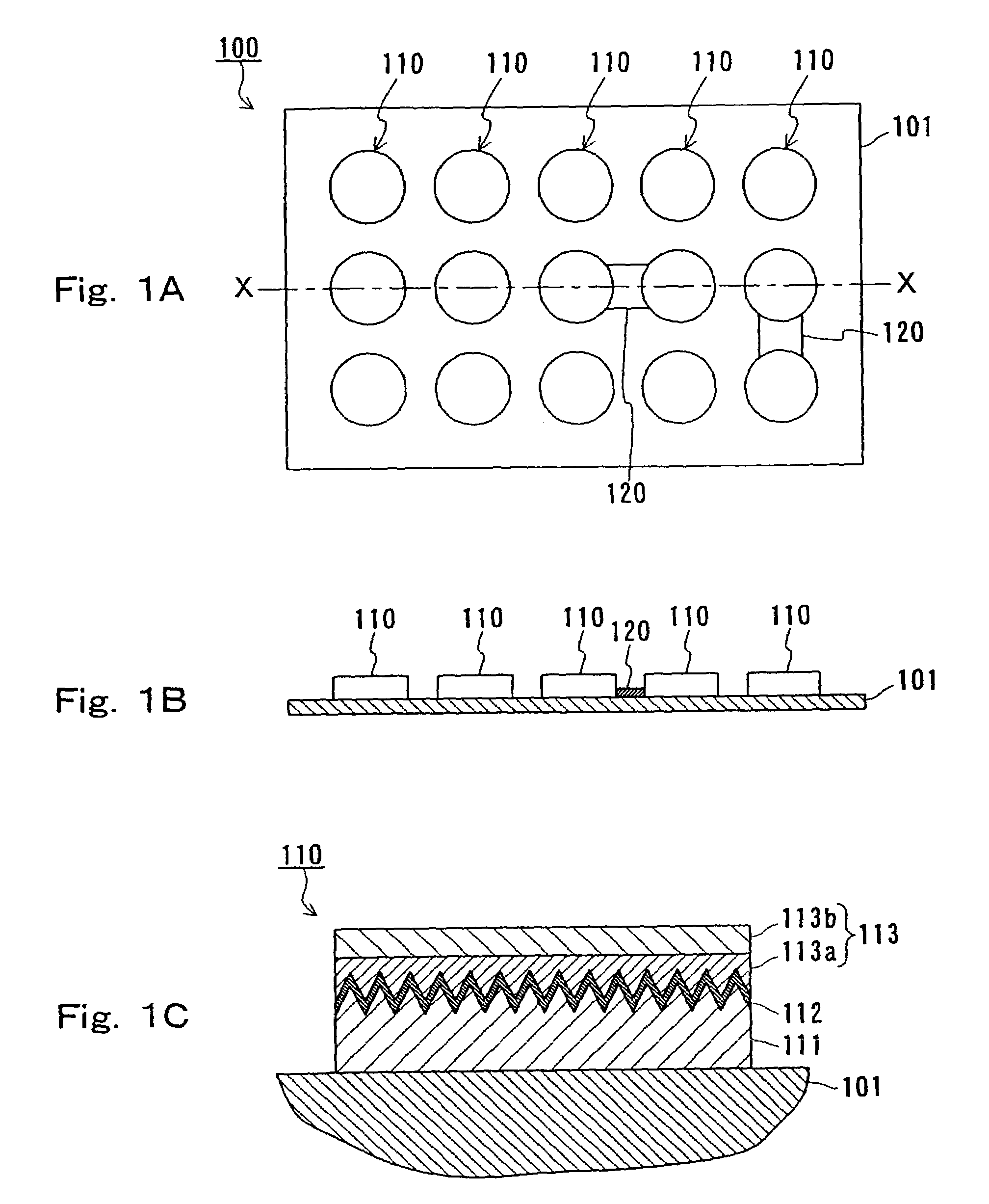
[0078]FIG. 1A is a plan view of a capacitor-mounted metal foil 100 in Embodiment 1, and FIG. 1B is a cross-sectional view taken along line X—X in FIG. 1A.
[0079]Referring to FIGS. 1A and 1B, the capacitor-mounted metal foil 100 includes a metal foil 101, a plurality of capacitors 110 (hatching is omitted) formed on the metal foil 101, and resistors 120. FIG. 1A shows a case where a plurality of capacitors 110 are arranged in a grid array shape; however, the capacitors 110 may be arranged in a different manner.
[0080]FIG. 1C shows an enlarged view of the capacitor 110. The capacitor 110 is a solid-state electrolytic capacitor. The capacitor 110 includes a metal layer 111, a dielectric layer 112, and a conductive layer 113 formed on the metal foil 101 in this order from the metal foil 101 side.
[0081]The metal foil 101 is made of, for example, a metal material forming a wiring p...
embodiment 2
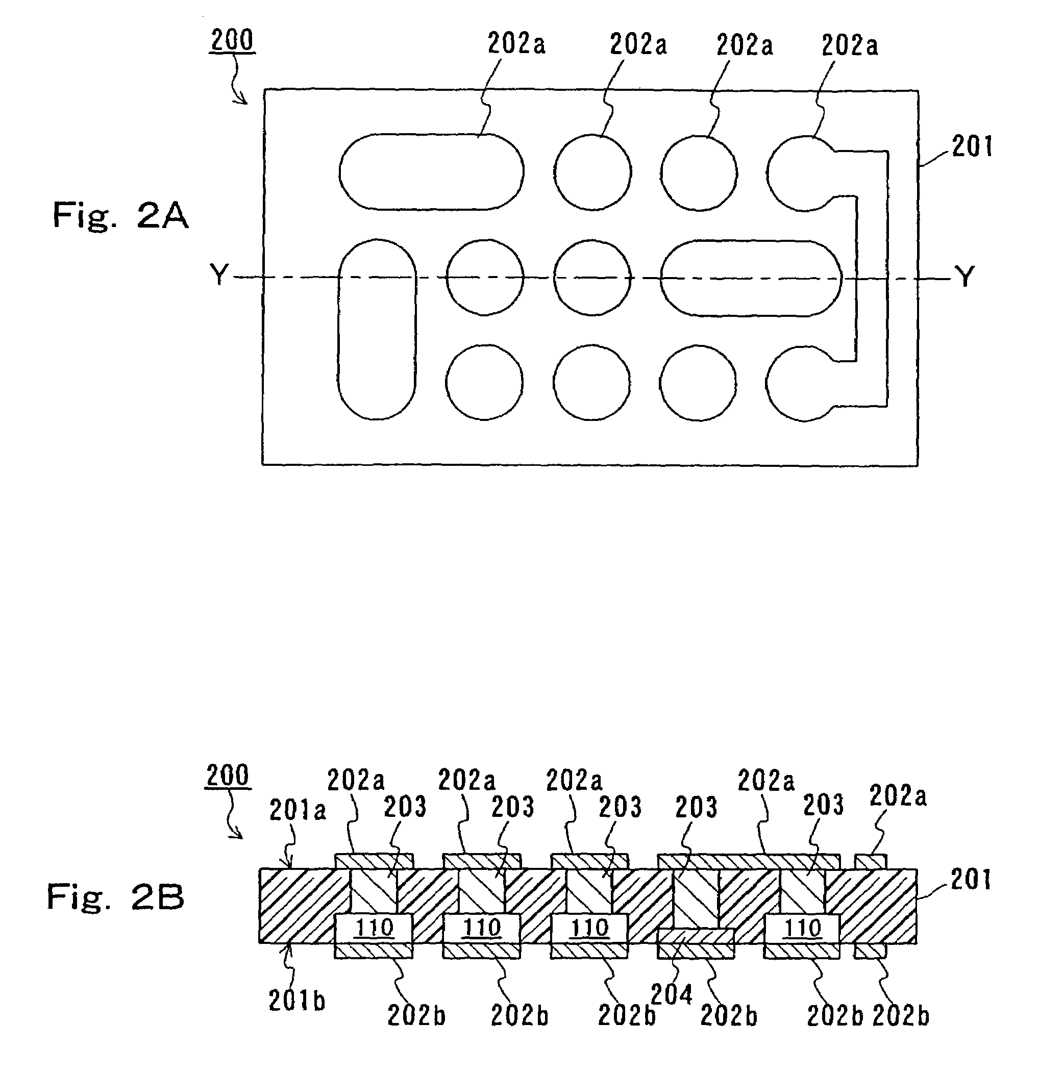
[0090]In Embodiment 2, an example of a circuit board of the present invention will be described. The same components as those in Embodiment 1 are denoted with the same reference numerals as those therein, and the description of the overlapping components will be omitted here (this also applies to the subsequent embodiments).
[0091]FIG. 2A shows a plan view of an example of a circuit board 200 in Embodiment 2, and FIG. 2B shows a cross-sectional view taken along line Y—Y in FIG. 2A.
[0092]Referring to FIGS. 2A and 2B, the circuit board 200 includes an insulating base 201, two wiring patterns 202a and 202b formed on two principal planes of the base 201, inner vias 203 formed in the base 201, and a plurality of capacitors 110 formed on the wiring pattern 202b. The capacitor 110 is the same as that described in Embodiment 1.
[0093]The base 201 is made of an insulating material. For example, the base 201 may be made of a thermosetting resin mixed with an inorganic filler (powder made of a i...
embodiment 3
[0098]In Embodiment 3, another example of a circuit board of the present invention will be described. The circuit board 300 in Embodiment 3 is different from that in Embodiment 2 in that three-layer wiring patters are provided. Therefore, the overlapping description will be omitted here.
[0099]FIG. 3 shows a cross-sectional view of the circuit board 300. Referring to FIG. 3, the circuit board 300 includes an insulating base 301, a plurality of wiring patterns 202a, 202b, and 302a, inner vias 203 formed in the base 301, and a plurality of capacitors 110 formed on the wiring pattern 202b. The circuit board 300 is obtained by layering an insulating base 301a on the circuit board 200 described in Embodiment 2 and forming the wiring pattern 302a thereon.
[0100]The circuit board 300 includes three-layer wiring patterns. The wiring patterns 302a and 202b are formed on two principal planes of the base 301. The wiring pattern 202a is disposed in the base 301.
[0101]The wiring pattern 302a is th...
PUM
| Property | Measurement | Unit |
|---|---|---|
| Dielectric polarization enthalpy | aaaaa | aaaaa |
| Electrical conductor | aaaaa | aaaaa |
| aaaaa | aaaaa |
Abstract
Description
Claims
Application Information