Forming an electrical contact on an electronic component

a technology of electrical contact and electronic component, which is applied in the direction of electrical equipment, climate sustainability, printed circuit aspects, etc., can solve the problems of increasing the difficulty of forming solder bumps by conventional methods, and increasing the difficulty of forming satisfactory connections of the required small size. , to achieve the effect of low resistance connections and high integrity

Inactive Publication Date: 2006-03-21
AGENCY FOR SCI TECH & RES
View PDF10 Cites 11 Cited by
  • Summary
  • Abstract
  • Description
  • Claims
  • Application Information

AI Technical Summary

Benefits of technology

[0010]It is an object of the present invention to provide a method of forming an electrical contact on an electronic component which enab...

Problems solved by technology

The use of such metal masks means that accurate alignment techniques are required to deposit the paste on individual pads and that the chance of bridging between pads increases as the pitch decreases.
It is becoming increasingly troublesome to form satisfactory connections ...

Method used


Image

  • Forming an electrical contact on an electronic component
  • Forming an electrical contact on an electronic component
  • Forming an electrical contact on an electronic component

Examples


Embodiment Construction

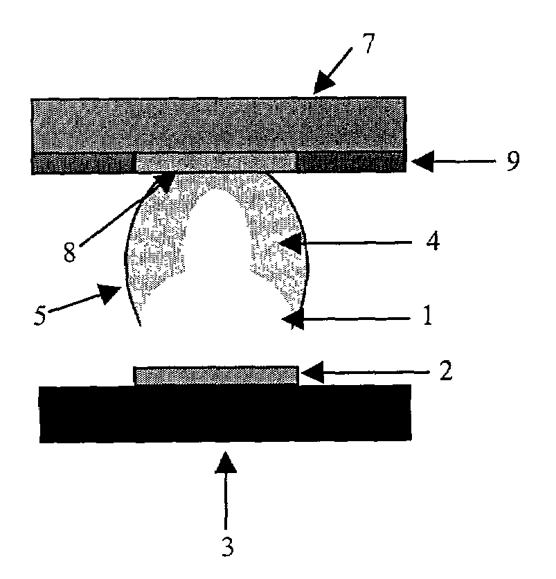
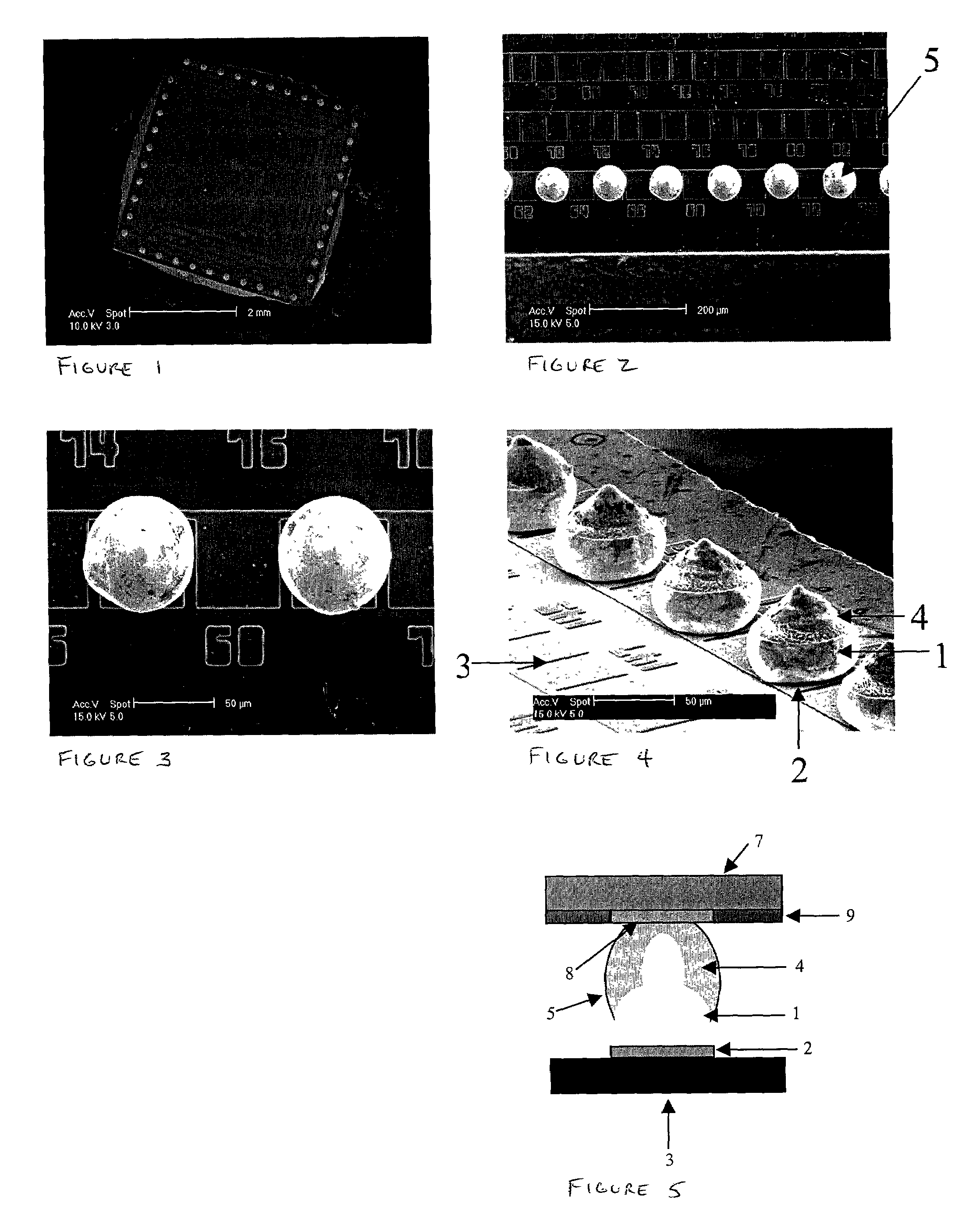
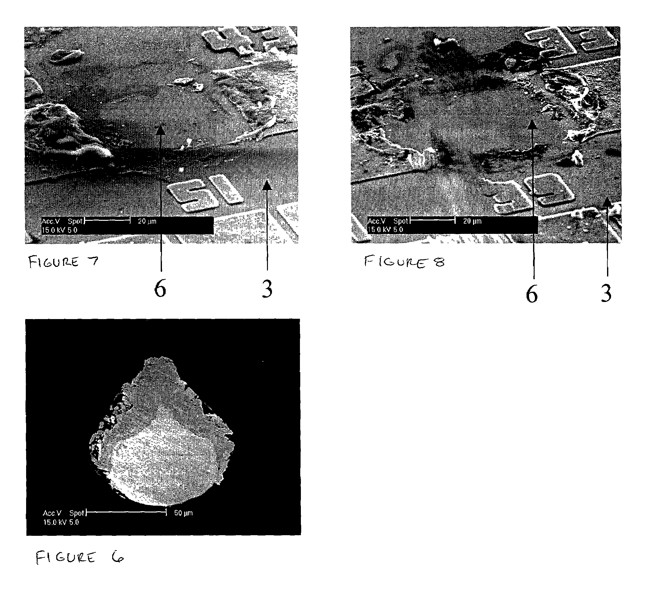
[0023]In one embodiment of the method of the present invention, protruding electrically conducting cores in the form of solid metal studs 1 (see FIGS. 4, 5 and 6) are fabricated on contact pads 2 of a semiconductor chip 3 which is to be electrically interconnected with a mounting substrate, which may be an organic substrate, in the manufacture of a packaged electronics product. The contact pads 2 are commonly made of aluminium or copper and may possibly be coated with other materials. The studs 1 are formed from gold wire of 25.4 μm diameter secured to the contact pads by means of a conventional wire bonding technique. The studs may be coined after they have been formed on the chip or may be left plain. Although the stud configurations shown in the drawings are linear arrays, both linear and two-dimensional stud arrays may be fabricated.

[0024]The projecting gold studs 1 thus formed on the contact pads 2 are then brought into contact with molten solder, for example by dipping in a so...


PUM


Abstract

A method of constructing an electrical contact on an electronic component comprises first forming a protruding electrically conducting stud at a contact location by wire bonding a metal wire to a contact pad of the component. The stud is then contacted with solder, without using a mask, so that a solder bump is deposited on and adheres to the metal stud to form a composite solder contact which is able to form with a contact of another component a solder joint which has good electrical and mechanical properties and which may be reliable fabricated at high density by a low cost method. An electronic component provided with such solder contacts and an electronics component package including such a component are also disclosed.

Description

RELATED APPLICATIONS[0001]This application claims priority to Singapore Application serial No. 200100049-6, filed Jan. 4, 2001, which is hereby incorporated by reference in its entirety.FIELD OF THE INVENTION[0002]This invention relates to a method of forming an electrical contact on an electronic component, such as the semiconductor chip or substrate of an electronic component package, particularly for application in flip-chip technology.BACKGROUND OF THE INVENTION[0003]With the increasing density of devices on a semiconductor chip and ever more complex applications there is a need to form ever smaller and more precise electrical connections when packaging such semiconductor chips, especially medium and higher end products with high input / output counts.[0004]In one conventional method, electrical connections in packaged electronic components are made using electrical contacts in the form of solder bumps which are deposited by a solder deposition process on contact pads of one of tw...

Claims


Application Information

Patent Timeline
IPC IPC(8): H01L21/44H01L21/60H01L23/485H01L23/498H05K3/34H05K3/40
CPCH01L23/49816H01L24/11H01L24/12H01L24/16H05K3/3436H01L2924/014H01L2924/01033H01L2924/00013H05K2203/049H05K2203/044H01L2224/1134H01L2224/131H01L2224/136H01L2924/01013H01L2924/01029H01L2924/01046H01L2924/01047H01L2924/01078H01L2924/01079H05K3/4015H05K2201/10242H01L2224/13099H01L2224/05568H01L2224/05573H01L2224/45144Y02P70/50H01L2924/00H01L2224/05624H01L2924/00014H01L2224/05647
Inventor LAHIRI, SYAMAL KUMARLEE, RINUS TEK POABU SAMAH, ZURUZI BIN
Owner AGENCY FOR SCI TECH & RES
Why Eureka
Try Eureka