
Abutted junction GMR read head with an improved hard bias layer and a method for its fabrication

a technology of hard bias layer and read head, which is applied in the field of fabrication of giant magnetoresistive (gmr) magnetic field sensor for magnetic read head, can solve the problems of current loss, electrical shorting between the lead and the shield, and the most serious impact on the stability of the sensor, so as to improve coercivity and squareness

Inactive Publication Date: 2006-03-21
HEADWAY TECH INC
View PDF8 Cites 24 Cited by
  • Summary
  • Abstract
  • Description
  • Claims
  • Application Information

AI Technical Summary

Benefits of technology

[0016]A first object of this invention is to provide a method for forming a hard (permanent) magnetic longitudinal bias layer for a spin-valve type abutted junction GMR sensor element which will produce a longitudinal bias layer with dramatically improved coercivity and squareness in the region of the abutted junction.
[0017]A second object of this invention into provide a method for forming a thinner hard magnetic bias layer, having the same magnetic moment as thicker bias layers of the prior art, for a spin-valve type abutted junction GMR sensor element, thus alleviating problems of electrical shorting between the sensor and the surrounding shields.

Problems solved by technology

The antiferromagnetic pinning layer and the NiFe underlayer found in many GMR sensors do not directly contribute to the GMR effect, but do contribute to current loss.
If the shields are then brought down too close to the conducting leads in an attempt to minimize thickness, the possibility of electrical shorting between the leads and the shields becomes a problem.
A disadvantage of this geometry is the fact that the sensor stability is then most seriously affected by the properties of the bias layer at the position of junction itself, particularly at the tail of the seed layer upon which the magnetic layers of the sensor element are formed.
The prior art of forming longitudinal bias layers, as evidenced by the patents cited above, does not adequately take into consideration the properties of the bias layer at the junction and the importance of achieving proper material matching thereat.

Method used


Image

  • Abutted junction GMR read head with an improved hard bias layer and a method for its fabrication
  • Abutted junction GMR read head with an improved hard bias layer and a method for its fabrication

Examples


Embodiment Construction

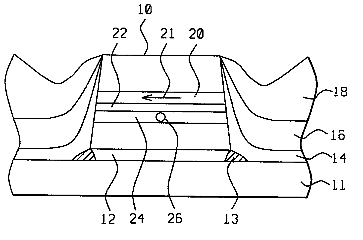
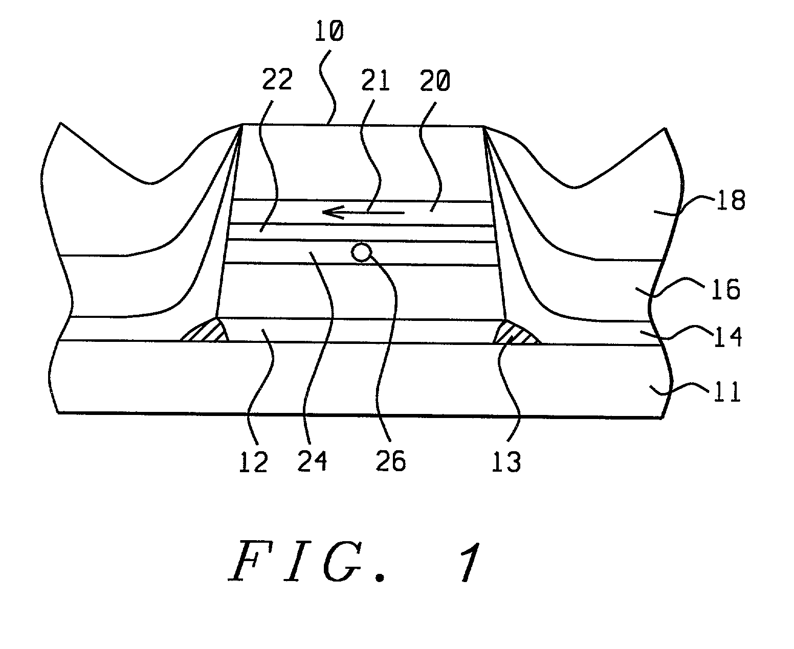
[0022]The present invention is a spin-valve type abutted junction GMR sensor element with a thinner hard magnetic longitudinal bias layer having significantly improved magnetic properties in the junction region. The fabrication of said GMR sensor element in accord with the preferred embodiment of the present invention is to be understood in the context of FIG. 1 and the description provided below.

[0023]Referring to FIG. 1, there is shown an abutted junction spin-valve type GMR sensor element fabricated in accordance with the methods of this invention. It comprises a spin-valve GMR sensor stack (10), upon whose abutted junction is formed a seed layer (14), composed of Cr, CrX or Ta / CrX alloy, where X can be any member of the group consisting of Ti, W, Mo, V or Mn. Said CrX seed layer is formed to a thickness of between 15 Angstroms and 200 Angstroms, whereas said Ta underlayer, upon which may be formed the CrX seed layer, is formed to a thickness of between 10 Angstroms and 200 Angst...


PUM

PropertyMeasurementUnit
Thicknessaaaaaaaaaa
Thicknessaaaaaaaaaa
Thicknessaaaaaaaaaa

Abstract

A method for forming a spin-valve type abutted junction GMR sensor element with a thinner hard magnetic longitudinal bias layer having significantly improved magnetic properties in the junction region and a spin-valve type abutted junction GMR sensor element with a thinner hard magnetic longitudinal bias layer having significantly improved magnetic properties in the junction region fabricated according to that method.

Description

BACKGROUND OF THE INVENTION[0001]1. Field of the Invention[0002]This invention relates generally to the fabrication of a giant magnetoresistive (GMR) magnetic field sensor for a magnetic read head, more specifically to the formation of magnetic bias layers on an abutted junction.[0003]2. Description of the Related Art[0004]Magnetic read heads whose sensors make use of the giant magnetoresistive effect (GMR) in the spin-valve configuration (SVMR) base their operation on the fact that magnetic fields produced by data stored in the medium being read cause the direction of the magnetization of one layer in the sensor (the free magnetic layer) to move relative to a fixed magnetization direction of another layer of the sensor (the fixed or pinned magnetic layer). Because the resistance of the sensor element is proportional to the cosine of the (varying) angle between these two magnetizations, a constant current (the sensing current) passing through the sensor produces a varying voltage ac...

Claims


Application Information

Patent Timeline
IPC IPC(8): G11B5/127G01R33/09G11B5/31G11B5/39
CPCB82Y10/00B82Y25/00G01R33/093G11B5/3903Y10T29/49032G11B5/3932G11B2005/3996G11B5/3163
Inventor CHIEN, CHEN-JUNGTORNG, CHYU-JIUHHAN, CHERNG-CHYIHORNG, CHENG T.CHEN, MAO-MIN
Owner HEADWAY TECH INC
Learn More