Functional pattern logic diagnostic method

a technology of functional failure and diagnostic method, which is applied in the field of diagnostic method of complex semiconductor devices, can solve the problems of time-consuming and difficult method of diagnosing devices that have failed functional testing, and the failure of functional testing is generally very difficult to diagnose, and the failure of functional testing is generally very difficult to achieve. , to achieve the effect of time-consuming and difficult to diagnos

Inactive Publication Date: 2006-03-21
IBM CORP
View PDF4 Cites 15 Cited by
  • Summary
  • Abstract
  • Description
  • Claims
  • Application Information

AI Technical Summary

Benefits of technology

[0015]Another object of the present invention is to allow for a systematic diagnostic methodology based on design structure rather than functional behavior, thereby reducing turn-around-time and fault localization accuracy and resolution.
[0017]The present invention especially accomplishes this by transforming a functional pattern into a scan deterministic pattern so that existing diagnostic tools can also be used without impacting manufacturing test.
[0023]As previously noted, functional fails are generally very difficult and time consuming to diagnose. The present invention avoids these difficulties by generating structural LSSD test patterns that will induce a failure mechanism that behaves in a similar failing manner.

Problems solved by technology

However this method of diagnosing of such complex logic structures to determine the devices that have failed functional testing is very time consuming and difficult and is even more difficult when the circuit designs are sequential in nature and utilize a functional pattern test methodology as found in LSSD circuits.
Functional fails are generally very difficult to diagnose since detail understanding of the logic circuit design and functional fail behavior is necessary and using the prior art techniques requires that test engineers and designers dedicate many hours and several diagnostic iterations to understand and diagnose the failure mechanism.
This basic problem complicates the diagnostic process by the need to track the structure's logical states for several previous events.

Method used


Image

  • Functional pattern logic diagnostic method
  • Functional pattern logic diagnostic method
  • Functional pattern logic diagnostic method

Examples


Embodiment Construction

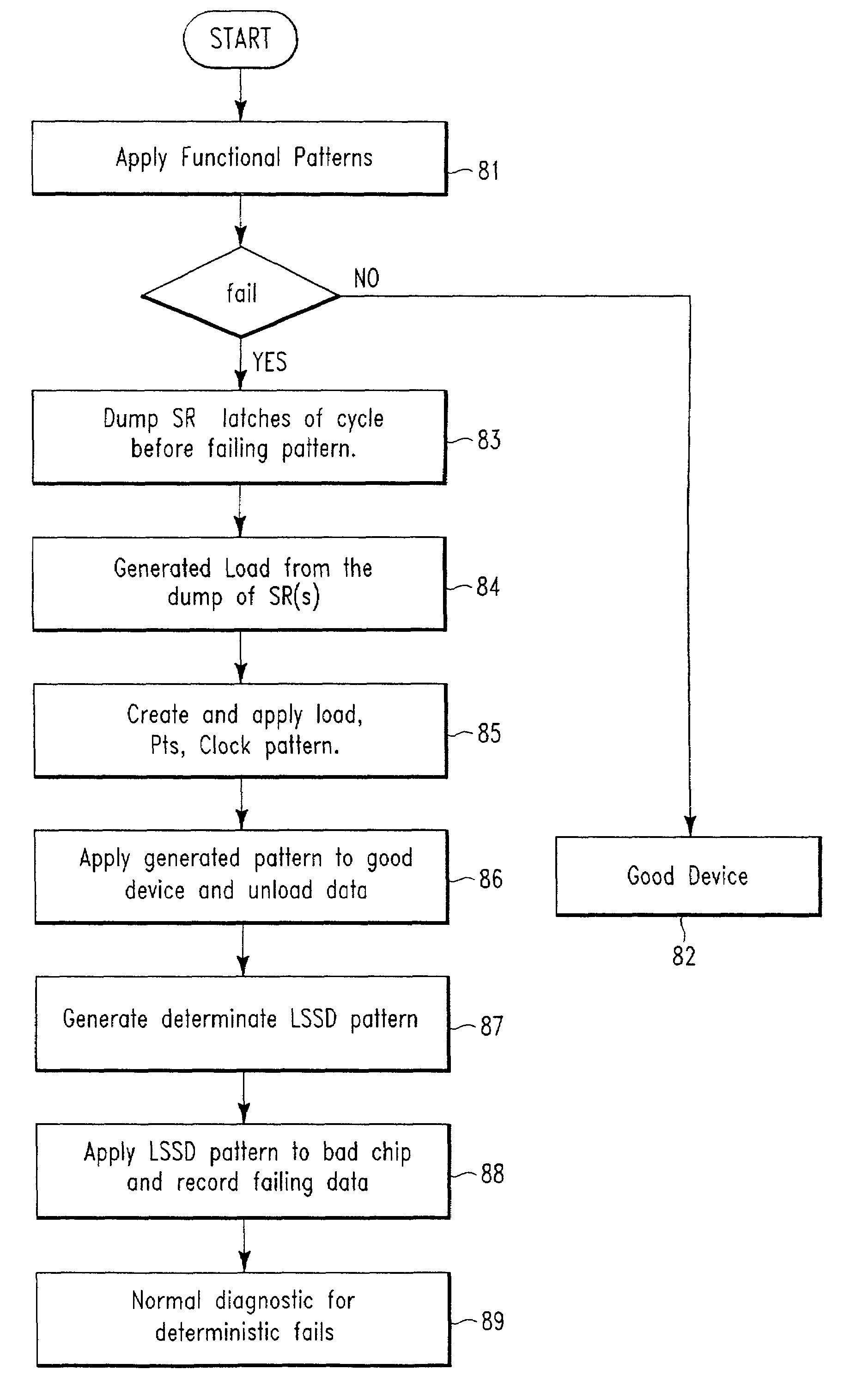
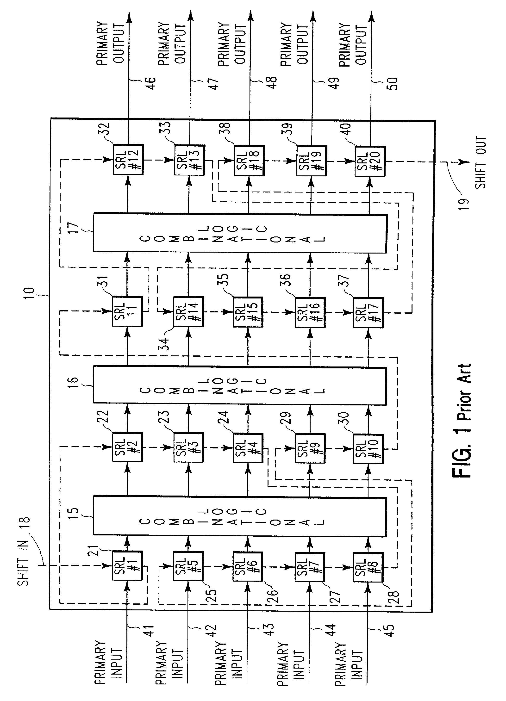
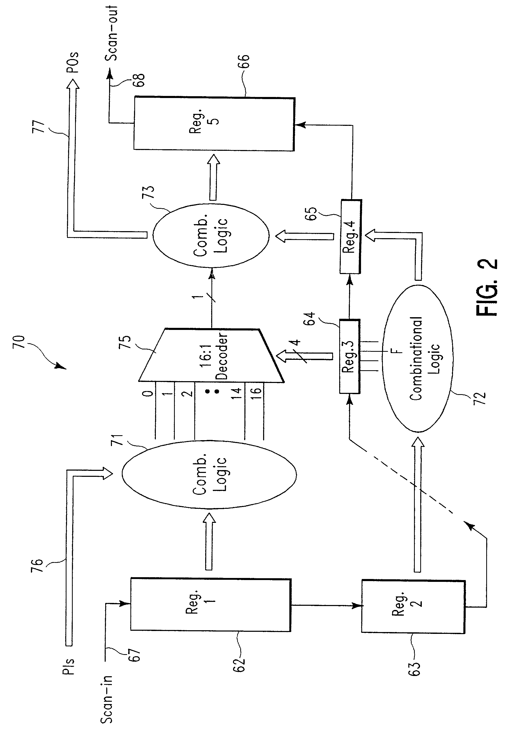
[0028]These and other features and advantages of the present invention will become more readily apparent from the following detailed description thereof, when read with reference to the accompanying drawings wherein FIG. 1 illustrates a typical digital logic chip having a linear distribution of primary input and primary output signal lines along the shift register scan string; FIG. 2 schematically illustrates the interaction between a selected number of shift register latches and the combinational logic of a logic chip having a failure therein tested and FIG. 3 is a flow chart illustrating the steps of the present invention.

[0029]FIG. 1 illustrates a typical digital logic chip 10 including combinational logic and a shift register scan string coupled between a SHIFT IN line 18, a SHIFT OUT line 19 and individual shift register latches 21 through 40. As is well known to the art, such combinational logic is comprised of a plurality of interconnected digital logic circuits and the activ...


PUM


Abstract

A method of diagnosing semiconductor device functional testing failures by combining deterministic and functional testing to create a new test pattern based on the functional failure by determining the location of and type of error in the failing circuit. This is accomplished by identifying the failing vector during the functional test, observing the states of the failed device by unloading the values of the latches from the LSSD scan chain before the failing vector, generating a LOAD from the unloaded states of the latches, applying the generated LOAD as the first event of a newly created independent LSSD deterministic pattern, applying the primary inputs and Clocks that produced the failure to a correctly operating device, unloading the output of the correctly operating device to generate a deterministic LSSD pattern; and applying the generated deterministic LSSD pattern to the failing device to diagnose the failure using existing LSSD deterministic tools.

Description

BACKGROUND OF THE INVENTION[0001]1. Field of the Invention[0002]This invention relates generally to a method of diagnosing complex semiconductor devices utilizing logic circuits that have failed functional testing. More particularly this invention diagnoses and determines the failing locations by combining functional testing of the device circuitry with structural design and test techniques to dynamically create a new test pattern based on the functional failure and thereby determine the location of and type of error in the failing circuit.[0003]2. Background of the Invention[0004]Level Sensitive Scan Design (LSSD) methodology is well known to the prior art. Basically the LSSD methodology is a system design in which the device under test has a plurality of storage elements, i.e., latches or registers, that are concatenated in one or more scan chains and are externally accessible via one or more serial inputs and outputs. Storage elements that are not so concatenated are usually memo...

Claims


Application Information

Patent Timeline
Patent Type & Authority Patents(United States)
IPC IPC(8): G01R31/28G06F11/00G01R31/3185
CPCG01R31/318586G01R31/318544
Inventor FORLENZA, DONATOMOTIKA, FRANCONIGH, PHILLIP J.
Owner IBM CORP
Why Eureka
Try Eureka